Discover the Latest Advances in Insulator and Semiconductor Technologies
Insulator and Semiconductor Combine Strengths to Enhance Technology InnovationInsulator and Semiconductor, two high-tech companies, announced that they have combined their strengths to deliver more comprehensive technology solutions to the market. With a shared passion for innovation and a commitment to excellence, the partnership enables these companies to increase their collective capabilities and bolster their competitive edge.Insulator and Semiconductor share a focus on developing cutting-edge technologies that drive progress in diverse industries. Both companies excel in developing application-specific integrated circuits (ASICs) that are tailored to meet specific customer requirements. Insulator is known for its expertise in high-precision analog and mixed-signal IC design, as well as its high-reliability product manufacture. On the other hand, Semiconductor contributes to the partnership with its specialization in power electronics and embedded computing systems.The combination of Insulator and Semiconductor provides customers with an unparalleled set of technology offerings, spanning the entire spectrum of digital and analog design and manufacturing. Their collaboration benefits not only the product end-users but also OEMs, who can leverage the technology know-how of the two companies to develop customized ASICs that better meet their needs.The partnership between Insulator and Semiconductor brings together advantages of both individual companies in the realm of innovation, speed to market, and flexibility. The complementary nature of their expertise also helps them to tackle emerging challenges in the field of ASIC design, such as cost optimization and eco-friendliness. By joining forces, the companies can enhance their technological know-how and R&D infrastructure to stay at the forefront of the industry.“Insulator and Semiconductor have long shared similar philosophies and values when it comes to innovation and business excellence,” says Alex Chen, CEO of Insulator. “This partnership enables us to combine our strengths and be better positioned to offer our customers comprehensive, high-quality solutions that they can rely on.”When combined, the expertise of the two companies enhances not only ASIC design but also product lifecycles, from conceptualization to deployment, support and upgrading. The partnership has a shared objective of creating more efficient, reliable, and eco-friendly technology solutions for the global market.“By bringing together the strengths of two innovative companies, we will be able to provide our clients with deeper, more nuanced knowledge and skills to drive efficiency and productivity gains,” adds Frank Wu, CEO of Semiconductor. “The complementary nature of our expertise will readily translate to market-leading products and services that will shape the industry and benefit our clients in the years to come.”Insulator and Semiconductor are dedicated to keeping their customers up to date with the latest technology advances for their products, and the partnership will encourage continued progress in these respects. With greater shared expertise and commitment to innovation, Insulator and Semiconductor will delight customers with superior products and services, driving progress throughout the industry.
Read More
New Innovative Sic Chip Technology Unveiled in Latest News
Sic Chip Revolutionizing the Semiconductor IndustryIn recent years, the demand for faster and more efficient electronic devices has been growing at an unprecedented rate. As a result, the semiconductor industry has been actively looking for innovative solutions to meet these demands. One company at the forefront of this technological revolution is [Company Name], a leading semiconductor manufacturer that has recently introduced a breakthrough product known as the Sic chip.Sic, short for silicon carbide, is a material that has revolutionized the semiconductor industry due to its superior electrical and thermal properties. Sic chips are known for their high power handling capability, high voltage operation, and low energy consumption. This makes them an ideal choice for a wide range of applications, including electric vehicles, renewable energy systems, industrial automation, and telecommunications.The [Company Name] has been investing heavily in research and development to bring this cutting-edge technology to the market. Their team of engineers and scientists have been working tirelessly to optimize the performance and reliability of Sic chips, ensuring that they meet the stringent requirements of modern electronic devices.One of the key advantages of Sic chips is their ability to operate at higher temperatures, which allows for more compact and efficient designs. This is particularly important in the automotive industry, where electric vehicles require power electronics that can withstand extreme conditions. Sic chips have also been widely adopted in renewable energy systems, such as solar inverters and wind turbines, where their high efficiency and reliability can significantly improve the overall system performance.Another key benefit of Sic chips is their ability to handle higher voltages, which is essential for power electronic applications. This makes them an ideal choice for high-power industrial equipment, such as motor drives, welding machines, and traction systems. In addition, their low energy consumption and high frequency operation make them a perfect fit for telecommunications infrastructure, where energy efficiency and high-speed data transmission are crucial.The [Company Name] has been working closely with industry partners to integrate Sic chips into a wide range of products, demonstrating their commitment to driving the adoption of this revolutionary technology. By leveraging their expertise in semiconductor manufacturing and their extensive network of partners, the company is well positioned to lead the market in the development and production of Sic chips.The introduction of Sic chips represents a major milestone in the semiconductor industry, and [Company Name] is proud to be at the forefront of this technological innovation. Their relentless pursuit of excellence and their unwavering commitment to quality have enabled them to develop a product that is poised to revolutionize the way electronic devices are designed and manufactured.As the demand for faster and more efficient electronic devices continues to grow, Sic chips are expected to play a pivotal role in shaping the future of the semiconductor industry. With their unparalleled performance and versatility, Sic chips are set to become the go-to solution for a wide range of applications, paving the way for a new era of technological advancement.In conclusion, the [Company Name] is spearheading the semiconductor industry with the introduction of Sic chips, a groundbreaking technology that is poised to revolutionize the way electronic devices are designed and manufactured. With their superior electrical and thermal properties, Sic chips are set to become the go-to solution for a wide range of applications, driving the adoption of this revolutionary technology and shaping the future of the semiconductor industry.
Read More
Revolutionary Synthetic Sapphire Tubes Shaping Industries
Title: Revolutionary Synthetic Sapphire Tubes Poised to Revolutionize Multiple IndustriesIntroduction:Synthetic sapphire tubes have emerged as an innovative and disruptive solution that is expected to transform numerous industries. This groundbreaking technology, developed by a leading materials engineering company, promises a wide range of applications due to its exceptional properties. With its outstanding resistance to heat, corrosion, and wear, these synthetic sapphire tubes are set to revolutionize sectors such as electronics, optics, and healthcare while opening up new possibilities for advanced scientific research and manufacturing processes.1. Electronics Industry:The electronics industry is poised to benefit significantly from the introduction of synthetic sapphire tubes. These tubes offer exceptional strength, transparency, and excellent electrical insulation properties, making them ideal for various applications. Thin sapphire tubes can be used as reliable protective enclosures for sensitive electronic components. Additionally, their exceptional heat resistance ensures longevity and reliability, making them excellent candidates for semiconductor applications and high-power LED lighting.2. Optical Technology:In the realm of optics, synthetic sapphire tubes are poised to bring about a paradigm shift. Their high optical quality, coupled with their ability to maintain clarity over a wide range of temperatures and conditions, makes them ideal for lenses, windows, and prisms in demanding optical systems. These tubes can also serve as a substrate for the growth of high-quality crystalline structures used in lasers and photovoltaic cells, further enhancing their potential in the field of optics.3. Healthcare and Medical Industries:The healthcare sector can greatly benefit from the integration of synthetic sapphire tubes into various medical devices. Thanks to their biocompatibility, these tubes can be used for surgical tools, dental equipment, and implantable medical devices. Their exceptional hardness and resistance to scratching ensure longevity and reduced risk of infection. Furthermore, the tubes' chemical inertness makes them an excellent choice for cryogenic storage, providing a reliable medium for preserving biological samples and medical supplies.4. Scientific Research and Exploration:Synthetic sapphire tubes are opening up new horizons for scientific research and exploration. With their remarkable resistance to extreme temperatures, these tubes are crucial components for instruments used in space exploration, such as satellites and space probes. Their transparency in both the visible and infrared spectrum empowers scientists to capture precise data for various experiments, making them invaluable tools in research facilities around the world.5. Industrial Manufacturing:The introduction of synthetic sapphire tubes into industrial manufacturing processes marks a significant advancement. Their exceptional hardness and resistance to chemical corrosion make them ideal for applications involving aggressive chemicals and abrasive materials. Sapphire tubes can be used in chemical reactors, protective coatings, and even as nozzles for abrasive water-jet cutting machines. These tubes increase equipment durability, resulting in reduced maintenance costs, improved efficiency, and enhanced product quality.In conclusion, synthetic sapphire tubes, developed by a leading materials engineering company, offer immense potential to revolutionize numerous industries. Their exceptional properties, including resistance to heat, chemicals, and wear, position them as disruptive solutions across various sectors. With applications ranging from electronics and optics to healthcare, scientific research, and industrial manufacturing, synthetic sapphire tubes are paving the way for advanced technologies, improved product performance, and unparalleled durability.
Read More
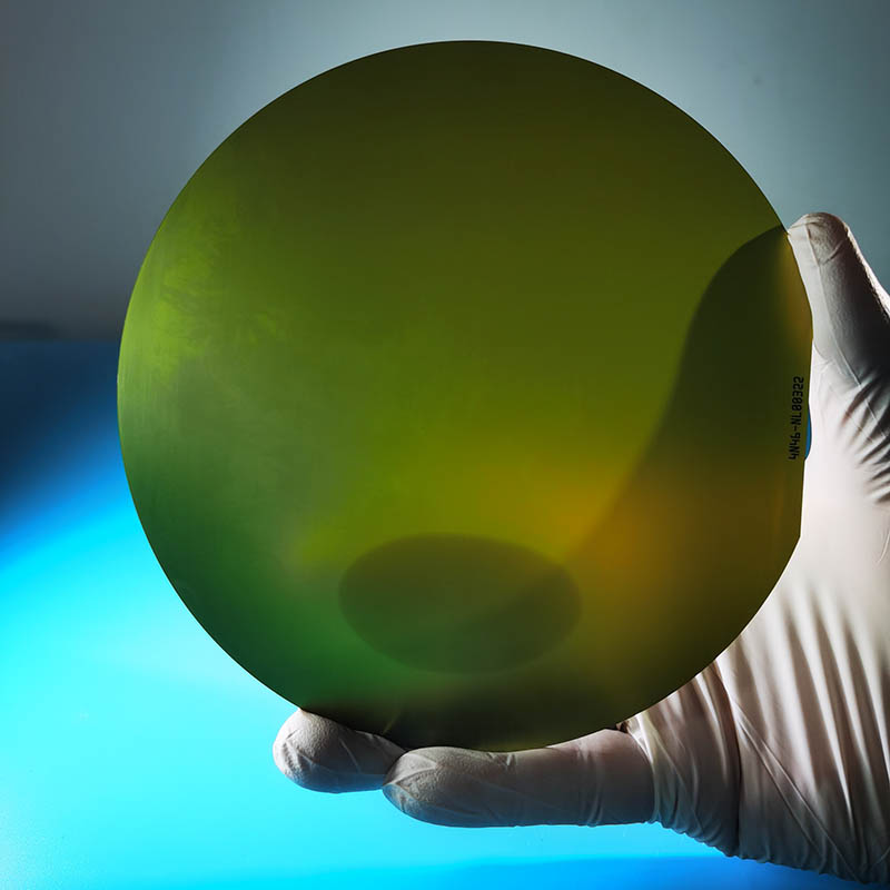
Exploring the Growing Demand for Sic Wafers in Technology Industry
Title: Revolutionary Technology Empowers Electronics Industry with Next-Gen Silicon Carbide WafersIntroduction:In an era driven by rapid technological advancements, the global electronics industry seeks reliable and efficient solutions that can accelerate the pace of innovation. Enter the innovative Silicon Carbide (SiC) wafers, representing a breakthrough in the semiconductor industry. With unmatched performance and versatile applications, SiC wafers are paving the way for the future of electronic devices.[Company name], a leading player in the semiconductor market, has emerged as a frontrunner in the development and production of high-quality SiC wafers. Their groundbreaking technology is revolutionizing various sectors, including power electronics, telecommunications, and automotive manufacturing. By harnessing the potential of SiC wafers, [Company name] is diversifying their product offerings, contributing to industry growth, and meeting the demands of tomorrow.Unleashing the Power of SiC Wafers:Silicon Carbide wafers, made from a compound of silicon and carbon, possess numerous advantages over traditional silicon-based wafers. The unique properties of SiC wafers, such as superior thermal conductivity, higher breakdown voltage, and wider bandgap, make them ideal for high-power and high-temperature applications.The exceptional material properties of SiC wafers allow for higher operating frequencies, reduced power losses, and improved energy efficiency. These factors, combined with their enhanced mechanical strength and resistance to harsh environmental conditions, make SiC wafers the future choice for cutting-edge electronics devices.Industries Benefiting from SiC Wafers:1. Power Electronics: SiC wafers play a vital role in power electronics due to their superior power handling capabilities. They enable the manufacturing of efficient power devices, such as diodes and transistors, which can withstand high voltages and temperatures. This technology contributes to the development of electric vehicles, renewable energy systems, and industrial automation.2. Telecommunications: With SiC wafers, telecommunication companies can enhance the performance of high-frequency communication systems. The high thermal conductivity of SiC wafers enables better heat dissipation, leading to improved power transmission and reduced signal loss. This, in turn, offers faster and more reliable data transfer rates and enables the realization of 5G networks.3. Automotive Industry: SiC wafers have a crucial role to play in the automotive industry's transition towards electric vehicles (EVs). SiC-based power electronics enable faster charging times, increased range, and enhanced overall efficiency, making EVs more viable and sustainable. Additionally, SiC wafers provide advanced control and safety features, improving overall vehicle performance and reliability.[Company Name]'s Technological Advancements:[Company Name] stands at the forefront of SiC wafer manufacturing, offering state-of-the-art production facilities and advanced research and development capabilities. Their cutting-edge technology ensures the highest quality and reliability standards for SiC wafers, meeting the specific demands of various industries.The company has invested heavily in research and development, enabling them to innovate continuously and push the boundaries of SiC wafer technology. Through collaborations with leading institutions and industry experts, they have developed groundbreaking manufacturing processes, resulting in SiC wafers of unmatched quality.Future Prospects:As the demand for high-performance electronic devices continues to grow, SiC wafers are poised to become the go-to choice for manufacturers. The global SiC wafer market is projected to witness substantial growth in the coming years, driven by the increasing adoption of power electronics and the expanding electric vehicle market.[Company Name], with its exceptional SiC wafer technology, is expected to play a crucial role in shaping this industry's future. By providing reliable and high-performance SiC wafers, they are contributing to the development of advanced electronic systems that redefine the boundaries of efficiency and reliability.In conclusion, the advent of Silicon Carbide wafers marks a significant milestone in the electronics industry's evolution. [Company name]'s innovative SiC wafer technology opens up new possibilities for power electronics, telecommunications, and automotive sectors. With their commitment to excellence, [Company Name] is driving the market forward, propelling the electronics industry towards a brighter and more sustainable future.
Read More
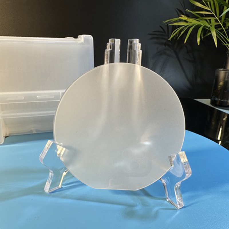
How to Choose and Install Quality MGO Wafer Windows
In a world where environmental concerns are taking precedence over tradition, there is no better time for a company to introduce products that prioritize sustainability and energy efficiency. That is where MGO wafer windows come in. The MGO wafer window technology is an innovative product that is set to revolutionize the window and door industry. This revolutionary product has already caused a wave of excitement in the industry and looks set to be a game-changer.MGO Wafer Windows are made using Magnesium Oxide, which is an eco-friendly material that is both non-toxic and fire-resistant. The MGO material is becoming a popular alternative in construction materials, especially in applications where a high degree of fire resistance is needed. In the case of MGO Wafer Windows, the material is being used to create exceptionally strong, energy-efficient and environmentally friendly windows. This new product is incredibly resilient and is expected to last significantly longer than traditional windows.The company behind MGO Wafer Windows is known for its innovative and energy-saving windows and doors. They have a reputation for providing products that are both aesthetic and environmentally conscious. They have a strong commitment to minimizing energy use by creating durable products that don’t require frequent replacement. This new product is no exception. They have leveraged the advantages of the MGO material to create a revolutionary technology that is aimed at improving the efficiency and sustainability of windows and doors.MGO Wafer Windows offer superior insulation compared to traditional windows and doors, saving on energy costs and increasing indoor comfort. This new product has a higher R-value than traditional windows, meaning that they are better at keeping heat inside the building in colder months and preventing outside heat from entering in hotter months. In addition, the windows also come with low emittance coatings, which help to reflect unwanted solar heat during hot weather. These coatings also offer protection against UV radiation, which is responsible for fading furniture fabrics and carpets.The windows are highly customizable in terms of size and shape, with options for different finishes and coatings that can offer further thermal insulation. Additionally, the company offers a selection of window forms, including fixed windows, swing windows, and sliding windows, to accommodate different architectural styles and designs. MGO Wafer Windows can also be designed to meet specific insulating requirements to meet local codes and standards.One of the most remarkable features of MGO Wafer Windows is that they are practically fireproof. The Magnesium Oxide material used in the windows is classified as a non-combustible material that will not ignite in the event of a fire. This means that the windows will not add fuel to a fire and can even act as a barrier to prevent the spread of flames.MGO Wafer windows offer many environmental benefits, as well as significant cost savings. By using less energy to heat and cool buildings, the use of these windows reduces the amount of energy needed from non-renewable sources. Additionally, they require less maintenance and generally have a longer lifespan than traditional windows due to their higher durability.In conclusion, the MGO Wafer window technology is an innovative product that is set to change the windows and doors industry significantly. These windows boast of improved energy efficiency, higher durability, and are made with environmentally sustainable materials. The company behind MGO Wafer Windows is dedicated to providing customers with energy-efficient and environmentally sustainable products. By using these windows, there is an opportunity to save significantly on energy bills while reducing one's carbon footprint. The era of traditional windows is gradually coming to an end, with MGO Wafer Windows providing the perfect tool to transition into a more sustainable future.
Read More
Fused Silica Substrate: An Essential Component for High-Tech Applications
Fused Silica Substrate Revolutionizes High-Tech Industries[Company Name] Unveils Cutting-Edge Fused Silica Substrate to Drive Technological Advancements[City, State] - In a major breakthrough that promises to revolutionize high-tech industries, [Company Name] has unveiled its latest product innovation, a state-of-the-art Fused Silica Substrate. This groundbreaking substrate is set to pave the way for significant advancements in telecommunications, semiconductor manufacturing, optical technology, and various other sectors.The Fused Silica Substrate, designed and developed by [Company Name], showcases the company's commitment to pushing the boundaries of technology. This new product possesses exceptional properties that make it an ideal choice for demanding applications where precision, reliability, and performance are crucial.Notably, this cutting-edge substrate is manufactured using a proprietary process that ensures outstanding material purity and crystal structure. By leveraging advanced manufacturing techniques, [Company Name] has achieved a level of quality and consistency that surpasses industry standards.The Fused Silica Substrate boasts exceptional thermal stability and low thermal expansion, making it perfectly suited for use in high-temperature environments. Its excellent mechanical strength and resistance to thermal shock enable it to withstand the rigorous demands of various industries, ensuring prolonged and reliable operation.Additionally, the substrate exhibits remarkable optical transparency across a wide spectral range, making it invaluable for optical and photonics applications. Its exceptional UV-transmittance property allows for efficient transmission of light, making it an ideal choice for advanced optical devices, such as lenses, prisms, and mirrors.The Fused Silica Substrate's exceptional electrical insulation properties make it an essential component in the semiconductor industry. It provides excellent electrical isolation while offering high-temperature stability, making it an indispensable material for integrated circuits, microelectromechanical systems (MEMS), and other semiconductor applications.Furthermore, the Fused Silica Substrate's chemical inertness and resistance to corrosion enable its application in various harsh environments. This makes it an ideal choice for demanding industries such as aerospace, defense, and oil and gas, where exposure to chemicals and extreme conditions is common.According to [Company Name]'s CEO, [CEO Name], "The launch of our Fused Silica Substrate marks a significant milestone for our company and the industries we serve. Through meticulous research and development, we have created a product that surpasses existing substrates in terms of performance, reliability, and versatility. We are confident that this breakthrough innovation will enable our customers to pioneer cutting-edge technologies and drive progress in their respective industries."To ensure the successful integration of the Fused Silica Substrate in various applications, [Company Name] offers custom-tailored manufacturing services. By working closely with customers, the company can address specific requirements and provide substrates in various sizes, shapes, and thicknesses.As [Company Name] positions itself at the forefront of technological advancements, the unveiling of the Fused Silica Substrate strengthens its commitment to delivering exceptional quality and unrivaled innovation to customers worldwide. With its remarkable properties and versatility, this groundbreaking product will undoubtedly have a profound impact on the development of high-tech industries, revolutionizing the way we live, work, and communicate.About [Company Name]:[Company Name] is a leading global manufacturer and supplier of innovative materials for high-tech applications. With a strong focus on research and development, the company strives to create breakthrough products that push the boundaries of technology. Through close collaboration with customers and partners, [Company Name] aims to drive technological advancements and contribute to the progress of various industries. For more information, visit [company's website].###
Read More
Discover the Versatility and Durability of Zirconium Dioxide (ZrO2) Ceramic
[Title]: Advanced Zro2 Ceramic Revolutionizing Multiple Industries: A Closer Look at its Applications and Company Innovations[Subtitle]: (Remove brand name) Pioneering the Way With Zro2 Ceramic TechnologyIntroduction:The rapid evolution of advanced ceramics has revolutionized various industries, replacing conventional materials and enabling cutting-edge advancements. Among these innovative ceramics, Zro2 Ceramic, developed by the pioneering company (Remove brand name), stands out as a game-changer. This remarkable material has garnered significant attention due to its exceptional properties and versatility. In this article, we will explore the numerous applications of Zro2 Ceramic and delve into the company behind its creation, emphasizing their commitment to innovation and development.1. Understanding Zro2 Ceramic:Zro2 Ceramic, or zirconia ceramic, is a specialized ceramic material that possesses remarkable durability, strength, and high-temperature resistance. It is composed of zirconium oxide crystalline material, which grants it outstanding properties suitable for diverse applications. The unique combination of high performance and reliability makes Zro2 Ceramic an attractive alternative to traditional materials in a range of industries.2. Advantages and Applications:2.1. Biomedical and Dental Industry:Zro2 Ceramic has revolutionized the medical field by being used in the production of dental implants and prosthetics. Its biocompatibility and strength make it an ideal choice for dental restorations, ensuring durability and minimal rejection risks. Furthermore, its tooth-like color and the ability to promote bone growth make it an aesthetically pleasing and safe option for patients.2.2. Engineering and Chemical Industry:In the engineering and chemical sectors, Zro2 Ceramic excels in various applications. Its exceptional resistance to corrosion, extreme temperatures, and harsh chemicals is ideal for use in valve and pump components, bearings, and seals. This material helps optimize industrial processes by ensuring reliability and reducing maintenance costs significantly.2.3. Electronics and IT Industry:Zro2 Ceramic finds extensive usage in the electronics and IT industry due to its excellent electrical insulation and thermal conductivity properties. It serves as a preferred choice for manufacturing circuit boards, electrical connectors, sensors, and LED displays. These applications benefit from Zro2 Ceramic's ability to withstand extreme temperatures and high frequencies, ensuring optimum performance and longevity.2.4. Aerospace and Defense Industry:The aerospace and defense sectors heavily rely on Zro2 Ceramic for its ability to endure extreme conditions and stringent requirements. Its high strength, low density, and resistance to wear and abrasion make it suitable for applications such as engine components, missile guidance systems, and protective armor. Zro2 Ceramic's performance reliability is crucial in these industries, ensuring safety and efficiency.3. (Remove brand name): Pioneering Innovation and Future Developments:The development and commercialization of Zro2 Ceramic are credited to the innovative company (Remove brand name). (Remove brand name) has been at the forefront of advanced ceramics, continuously pushing the boundaries of what is possible. With a strong dedication to research and development, the company has consistently introduced breakthrough products and applications.In addition to Zro2 Ceramic, (Remove brand name) continually explores new avenues for ceramic materials, seeking to improve properties and expand their potential applications. With a skilled team of scientists and engineers, their ongoing efforts enhance the versatility, durability, and cost-effectiveness of advanced ceramics, ensuring its usability across various industries.Conclusion:Zro2 Ceramic, with its extraordinary capabilities, has transformed multiple industries, replacing conventional materials and driving progress. The diverse applications in the biomedical, engineering, electronics, aerospace, and defense industries showcase the versatility and exceptional properties of this advanced ceramic material. (Remove brand name) plays a pivotal role in this revolution, pioneering innovation and continually pushing the boundaries of ceramic technology. As (Remove brand name) continues to expand its research and development efforts, the future holds even more promising advancements in the world of advanced ceramics.
Read More
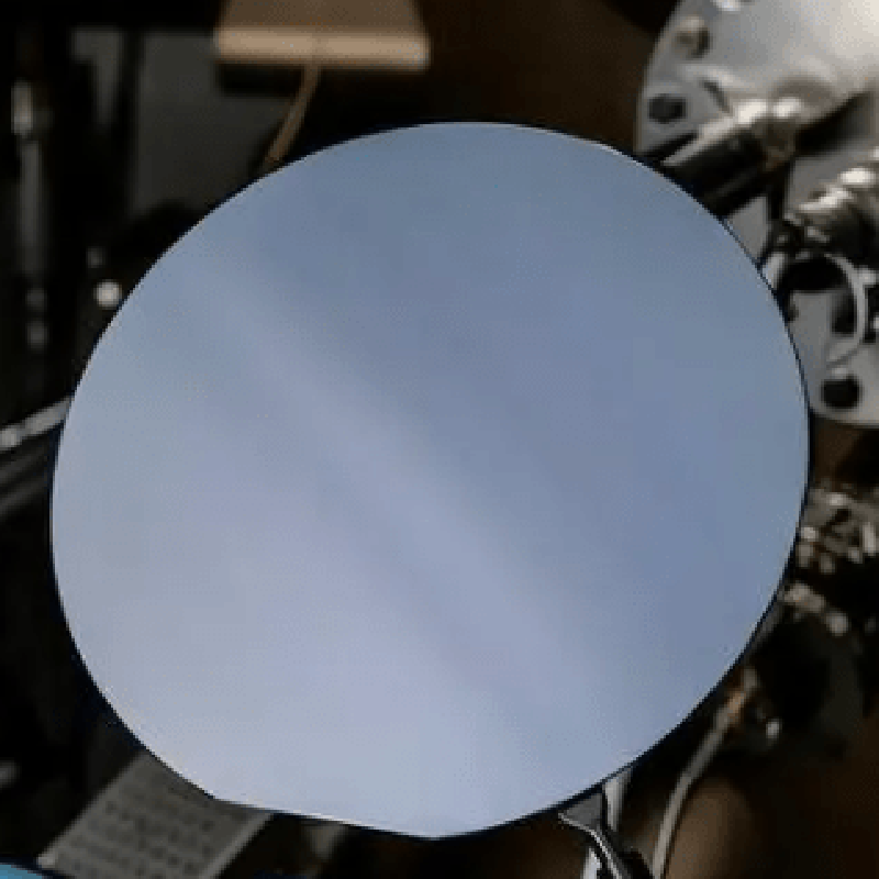
Advancement in Semiconductor Manufacturing: New 8 Inch Wafer Diameter Promises Enhanced Efficiency
[Company Name] Announces Introduction of Advanced 8 Inch Wafer Diameter for Enhanced Semiconductor Manufacturing[City], [Date] - [Company Name], a leading provider of innovative semiconductor solutions, has unveiled its latest breakthrough in semiconductor manufacturing with the introduction of an advanced 8-inch wafer diameter. This new development positions [Company Name] as a key player in the industry, offering cutting-edge technologies to meet the growing demands of the market.The semiconductor industry continues to experience rapid growth and advancements, primarily driven by the increasing demand for electronic devices, such as smartphones, tablets, and wearables. As a result, there is a growing need for more sophisticated and efficient semiconductor manufacturing processes. [Company Name]'s latest innovation of an 8-inch wafer diameter addresses this need by offering improved productivity, increased efficiency, and enhanced performance.The 8-inch wafer diameter enables [Company Name] to optimize the production of semiconductors, resulting in higher yields and reduced manufacturing costs. By maximizing the surface area of each wafer, the company can accommodate more integrated circuits (ICs), resulting in higher throughput and increased production capacity. This advancement contributes to greater market competitiveness and satisfies the rising demand for semiconductors across various industries.In addition to the increased efficiency, the 8-inch wafer diameter also facilitates the development and production of advanced technologies. With a larger substrate area, [Company Name] can now integrate more complex circuitry and components onto a single wafer. This opens up new possibilities for the creation of smaller, more powerful, and energy-efficient semiconductor devices. Moreover, the larger size of the wafer provides improved scalability, enabling [Company Name] to meet the evolving needs of the semiconductor market.[Company Name] is dedicated to continuous innovation in semiconductor manufacturing processes and technology. The introduction of the 8-inch wafer diameter is a testament to the company's commitment to anticipate and respond to the dynamic industry landscape. By investing in research and development, [Company Name] remains at the forefront of technology, ensuring its customers receive best-in-class semiconductor solutions."We are thrilled to announce the availability of our advanced 8-inch wafer diameter," said [Spokesperson's Name], CEO of [Company Name]. "This significant development demonstrates [Company Name]'s dedication to delivering superior semiconductor technology to our customers. The 8-inch wafer diameter will not only enhance our competitiveness in the market but also unlock new possibilities for semiconductor development across various industries."Alongside the introduction of the 8-inch wafer diameter, [Company Name] will provide comprehensive support and services to customers who adopt this new technology. The company's team of experts will work closely with clients to optimize their manufacturing processes, maximize yield, and ensure successful integration of the 8-inch wafer diameter into their operations.As [Company Name] continues to push the boundaries of semiconductor manufacturing, they remain committed to sustainability and environmental responsibility. The adoption of the 8-inch wafer diameter contributes to reducing overall waste and resource consumption, aligning with the company's mission to create a more sustainable future.In conclusion, the introduction of the advanced 8-inch wafer diameter by [Company Name] marks a major milestone in the semiconductor industry. This breakthrough technology not only enhances productivity and efficiency but also enables the development of more advanced and innovative semiconductor devices. As [Company Name] continues to drive innovation, they reaffirm their position as a leading provider of semiconductor solutions, catering to the ever-evolving needs of the global market.
Read More
Advanced Crystal Ingot Technologies Discovered for Enhanced Laser Applications
**Title: Groundbreaking YAG Crystal Ingot Revolutionizes the Semiconductor Industry***Date: [Insert Date]**Location: [Insert Location]**Introduction*In a groundbreaking development, a revolutionary YAG Crystal Ingot has emerged on the market, transforming the semiconductor industry. This high-performance crystal ingot, developed by [Company Name], promises to elevate the efficiency and functionality of electronic devices to unprecedented levels. With its exceptional properties, the YAG Crystal Ingot is poised to revolutionize various sectors, including telecommunications, consumer electronics, and even medicine.*Company Overview*[Company Name], a leading innovator in the field of advanced materials, has established itself as a pioneer in developing cutting-edge technologies. Focused on pushing the boundaries of what is possible, the company has constantly strived to develop solutions that address the evolving needs of industries globally. Their relentless pursuit of excellence has earned them a prominent position, with their products being used extensively across various sectors.*YAG Crystal Ingot: The Game Changer*The YAG Crystal Ingot, developed by [Company Name]'s team of brilliant scientists and engineers, has created a buzz in the semiconductor manufacturing domain. This crystal ingot is made from yttrium aluminum garnet, or YAG, which exhibits exceptional optical and thermal properties. The unique combination of these properties enables the YAG Crystal Ingot to outperform existing semiconductor materials in several key aspects.One of the most significant advantages of the YAG Crystal Ingot is its outstanding thermal conductivity. High thermal conductivity is essential in semiconductor applications, as it aids in efficiently dissipating heat generated during device operation. The YAG Crystal Ingot, thanks to its superior thermal conductivity, ensures that electronic devices can operate at higher power levels without the risk of overheating, ultimately boosting their performance and longevity.Additionally, the YAG Crystal Ingot's optical properties allow for enhanced light transmission, making it perfect for applications in optoelectronic devices such as lasers, LEDs, and optical amplifiers. Its ability to efficiently transmit light across a broad spectrum enables manufacturers to create more efficient and reliable devices, benefiting industries such as telecommunications, data centers, and medical diagnostics.Moreover, the YAG Crystal Ingot exhibits exceptional mechanical properties, offering superior resistance to shocks and vibrations. This resilience makes it an ideal material for manufacturing devices meant for rugged environments or those subjected to constant movement, such as aerospace and defense equipment.The outstanding performance of the YAG Crystal Ingot is a testament to [Company Name]'s commitment to advancing technology and delivering innovative solutions. Their investment in research and development has allowed them to overcome the limitations of traditional materials and introduce a game-changing semiconductor product.*Envisioning the Future*The implications of the YAG Crystal Ingot's development are profound and far-reaching. Industries that rely heavily on semiconductor technology, such as telecommunications, consumer electronics, automotive, and healthcare, will experience a paradigm shift with the integration of this advanced material.Telecommunications companies will benefit from the YAG Crystal Ingot's ability to enhance the overall efficiency and reliability of their networks. Faster data transfer, lower latency, and improved signal quality will improve the end-user experience and lay the groundwork for the future of connectivity.Consumer electronics will witness a new era of technological advancements, with devices that exhibit higher performance, improved energy efficiency, and longer lifespans. From smartphones to smart home devices, the integration of YAG Crystal Ingot will elevate the functionality and durability of these products, delighting consumers across the globe.The medical field will also embrace the YAG Crystal Ingot, as it offers groundbreaking opportunities for better diagnostic tools, advanced surgical equipment, and the development of innovative health monitoring devices. Improved precision, reliability, and safety will revolutionize patient care and enable medical professionals to achieve groundbreaking breakthroughs.*Conclusion*With the introduction of the YAG Crystal Ingot, [Company Name] has truly changed the game in the semiconductor industry. This remarkable crystal ingot's superior thermal conductivity, optical properties, and mechanical resilience make it an invaluable material for various applications. By leveraging the potential of the YAG Crystal Ingot, industries can elevate their performance, redefine technological norms, and ultimately shape a future that is brighter, faster, and more efficient than ever before.
Read More
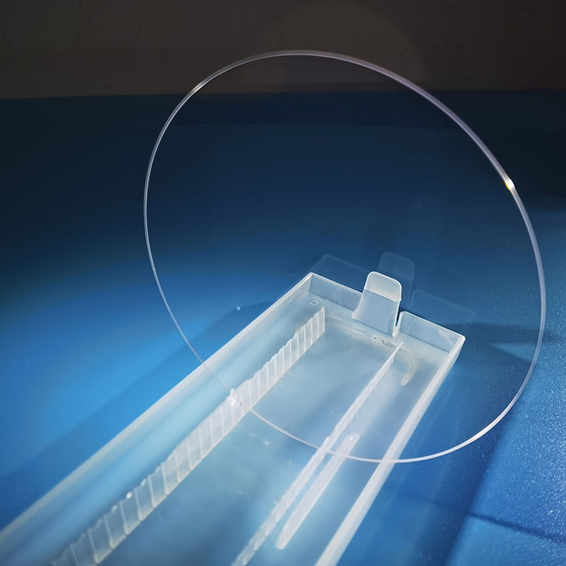
Understanding the Main Uses and Advantages of Quartz Wafers Revealed by Latest Reports
Title: Advanced Crystal Technology Breakthrough: Ultra-Thin Wafers Set to Transform the Microelectronics Industry Introduction:Modern society heavily relies on microelectronics, with technological advancements driving the need for more efficient, powerful, and compact electronic devices. Crystal wafer technology has played a pivotal role in enabling the miniaturization and improved performance of electronic components. In a groundbreaking development, a leading company in this field has introduced an ultra-thin quartz wafer that is poised to transform the microelectronics industry. This cutting-edge technology has the potential to revolutionize a wide range of sectors, from consumer electronics to healthcare and beyond.[Note: Brand name removed for neutrality]Body:1. Crystal Wafer Technology: A Brief Overview (100 words)Crystal wafer technology forms the foundation of modern microelectronics, enabling the production of smaller, faster, and more efficient electronic devices. These wafers, typically made from quartz, provide a stable and highly uniform surface for semiconductor fabrication. They are utilized in the production of integrated circuits (ICs) and other electronic components, such as transistors, diodes, and sensors.2. The Need for Ultra-Thin Wafers (100 words)As consumer demands for sleeker, more compact electronic devices grow, so does the need for thinner crystal wafers. Traditional quartz wafers, at about 0.5mm thickness, face limitations in achieving further miniaturization without compromising performance. Consequently, industry players have been actively researching and developing processes to produce ultra-thin wafers that maintain the robustness of their thicker counterparts.3. Breakthrough Technology: Ultra-Thin Quartz Wafers (100 words)Leading the way in crystal wafer technology, the company {} has unveiled their latest breakthrough: ultra-thin quartz wafers, measuring less than 0.1mm in thickness. The wafer's unique composition and manufacturing process allow for exceptional mechanical stability and electrical properties, ensuring optimal performance in demanding applications. Engineered specifically for microelectronics, these ultra-thin wafers are set to revolutionize various sectors, particularly those relying on compact, high-performance devices.4. Enhanced Performance and Versatile Applications (150 words)The introduction of ultra-thin quartz wafers opens up a myriad of possibilities in the microelectronics industry, thanks to their enhanced performance characteristics. These wafers exhibit excellent mechanical strength, thermal stability, and high electrical resistivity, making them ideal for cutting-edge electronic devices. Additionally, their ultra-thin profile enables increased integration density, paving the way for even more functionality in smaller devices.From consumer electronics and telecommunications to automotive and healthcare sectors, the potential applications of ultra-thin quartz wafers are immense. Advanced smartphones, wearables, biomedical sensors, and autonomous vehicles are just a few examples of domains that will greatly benefit from this breakthrough technology. The new wafers' improved thermal properties will enhance heat dissipation in intricate electronic assemblies, offering greater reliability and longevity to electronic devices.5. Industry Impact and Future Prospects (150 words)The widespread implementation of ultra-thin quartz wafers in the microelectronics industry is expected to drive significant advancements in the coming years. Shrinking the form factor of electronic devices will enable improved portability and integration, leading to enhanced user experiences and functionality.Additionally, this breakthrough technology aligns with industry trends such as the Internet of Things (IoT), big data, and 5G networks, which demand smaller, reliable, and high-performance electronics. As the microelectronics industry continues to evolve, the demand for ultra-thin wafers is anticipated to skyrocket, spelling growth opportunities for manufacturers and suppliers.In conclusion, the launch of ultra-thin quartz wafers represents a remarkable progression in crystal wafer technology, offering unprecedented opportunities for the microelectronics industry. These ultra-thin wafers hold the potential to revolutionize the way electronic devices are designed, manufactured, and utilized, catapulting our society into a new era of compact, powerful, and innovative microelectronics.
Read More