200mm 8inch GaN on sapphire Epi-layer wafer substrate
200mm 8inch GaN on sapphire Epi-layer wafer substrate
Shop for high-quality 200mm GaN on sapphire Epi-layer wafer substrates at our factory. We provide reliable products with superior performance and durability.
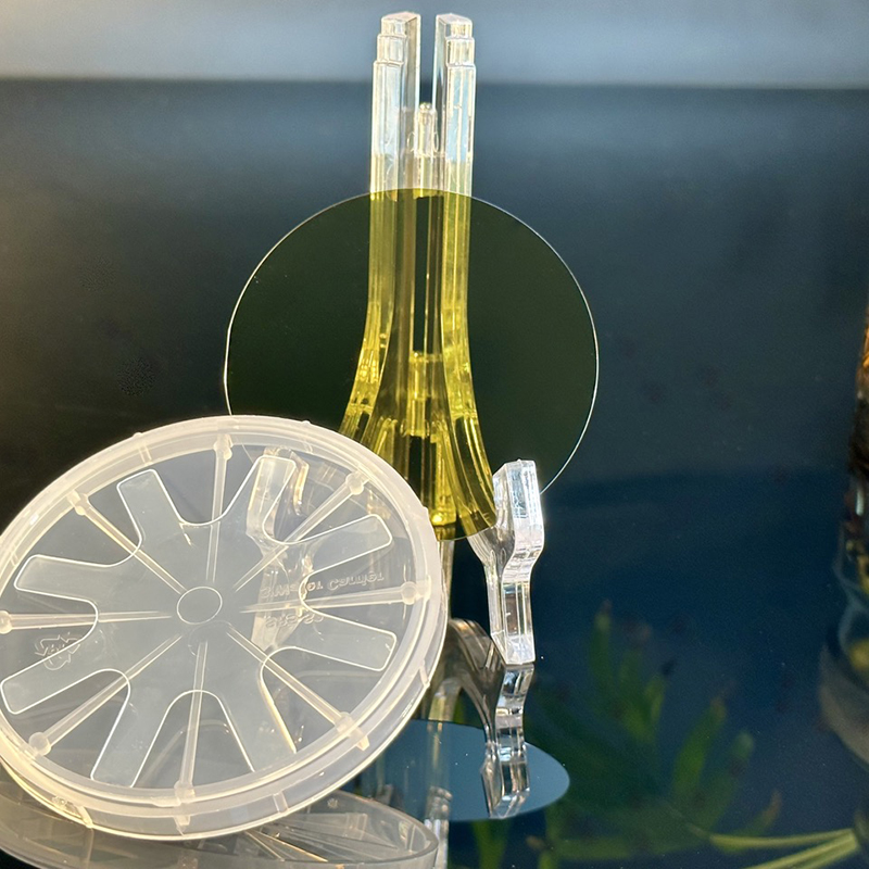
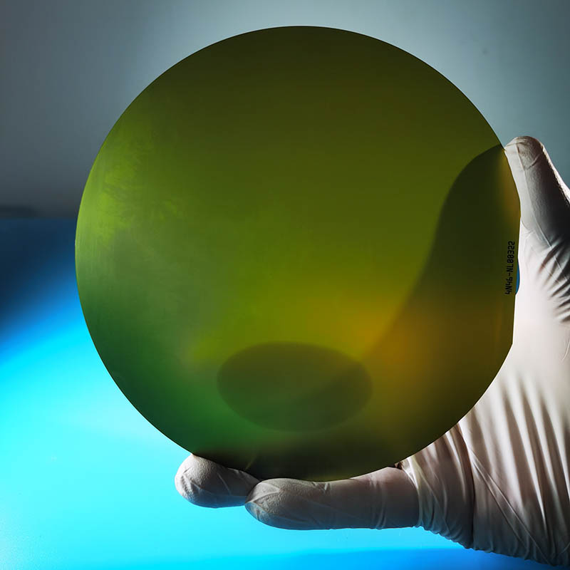
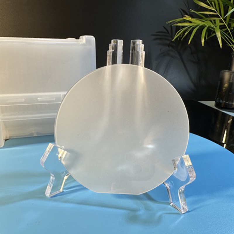
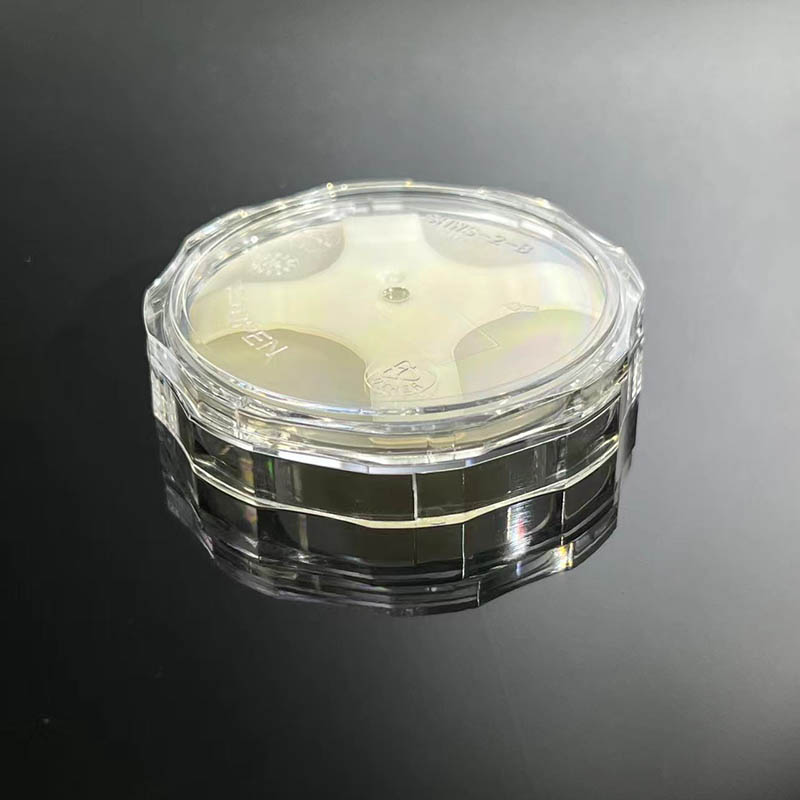
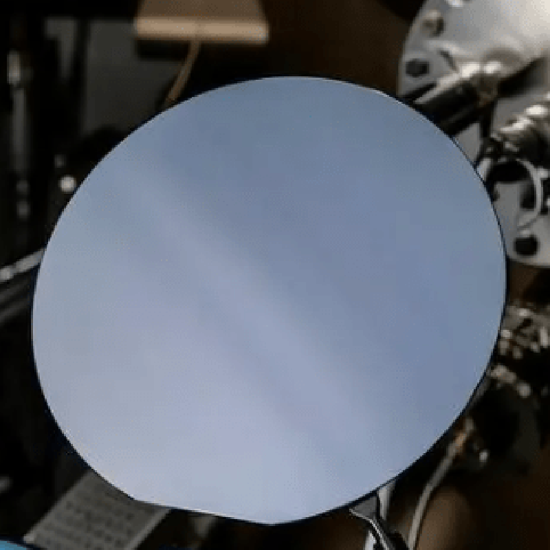
The 8-inch GaN-on-Sapphire substrate is a high-quality semiconductor material composed of a Gallium Nitride (GaN) layer grownon a Sapphire substrate. This material offers excellent electronic transport properties and is ideal for the fabrication of high-powerand high-frequency semiconductor devices. The manufacturing process involves the epitaxial growth of a GaN layer on a Sapphire substrate using advanced techniques suchas metal-organic chemical vapor deposition (MOCVD) or molecular beam epitaxy (MBE). The deposition is carried out under controlled conditions to ensure high crystal quality and film uniformity. The 8-inch GaN-on-Sapphire substrate finds extensive applications in various fields including microwave communications, radarsystems, wireless technology, and optoelectronics. Some of the common applications include: 1. RF power amplifiers 2. LED lighting industry 3. Wireless network communication devices 4. Electronic devices for high-temperature environments 5. Optoelectronic devices -Dimension: The substrate size is 8 inches (200 mm) in diameter. - Surface Quality: The surface is polished to a high degree of smoothness and exhibits excellent mirror-like quality. - Thickness: The GaN layer thickness can be customized based on specific requirements. - Packaging: The substrate is carefully packaged in anti-static materials to prevent damage during transit. - Orientation Flat: The substrate has a specific orientation flat to aid in wafer alignment and handling during device fabricationprocesses. - Other parameters: The specifics of the thickness, resistivity, and dopant concentration can be tailored as per customer requirements. With its superior material properties and versatile applications, the 8-inch GaN-on-Sapphire substrate is a reliable choice for thedevelopment of high-performance semiconductor devices in various industries.Except GaN-On-Sapphire, we also can offer in the field of power device applications, the product family includes 8-inch AlGaN/GaN-on-Si epitaxial wafers and 8-inch P-cap AlGaN/GaN-on-Si epitaxial wafers. At the same time, we innovated the application of its own advanced 8-inch GaN epitaxy technology in the microwave field, and developed an 8-inch AlGaN/ GAN-on-HR Si epitaxy wafer that combines high performance with large size, low cost and compatible with standard 8-inch device processing. In addition to silicon-based gallium nitride, we also have a product line of AlGaN/GaN-on-SiC epitaxial wafers to meet customers' needs for silicon-based gallium nitride epitaxial materials.


 The manufacturing process involves the epitaxial growth of a GaN layer on a Sapphire substrate using advanced techniques suchas metal-organic chemical vapor deposition (MOCVD) or molecular beam epitaxy (MBE). The deposition is carried out under controlled conditions to ensure high crystal quality and film uniformity. The 8-inch GaN-on-Sapphire substrate finds extensive applications in various fields including microwave communications, radarsystems, wireless technology, and optoelectronics. Some of the common applications include: 1. RF power amplifiers 2. LED lighting industry 3. Wireless network communication devices 4. Electronic devices for high-temperature environments 5. Optoelectronic devices -Dimension: The substrate size is 8 inches (200 mm) in diameter. - Surface Quality: The surface is polished to a high degree of smoothness and exhibits excellent mirror-like quality. - Thickness: The GaN layer thickness can be customized based on specific requirements. - Packaging: The substrate is carefully packaged in anti-static materials to prevent damage during transit. - Orientation Flat: The substrate has a specific orientation flat to aid in wafer alignment and handling during device fabricationprocesses. - Other parameters: The specifics of the thickness, resistivity, and dopant concentration can be tailored as per customer requirements. With its superior material properties and versatile applications, the 8-inch GaN-on-Sapphire substrate is a reliable choice for thedevelopment of high-performance semiconductor devices in various industries. Except GaN-On-Sapphire, we also can offer in the field of power device applications, the product family includes 8-inch AlGaN/GaN-on-Si epitaxial wafers and 8-inch P-cap AlGaN/GaN-on-Si epitaxial wafers. At the same time, we innovated the application of its own advanced 8-inch GaN epitaxy technology in the microwave field, and developed an 8-inch AlGaN/ GAN-on-HR Si epitaxy wafer that combines high performance with large size, low cost and compatible with standard 8-inch device processing. In addition to silicon-based gallium nitride, we also have a product line of AlGaN/GaN-on-SiC epitaxial wafers to meet customers' needs for silicon-based gallium nitride epitaxial materials.