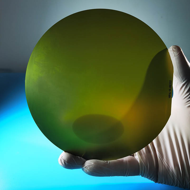
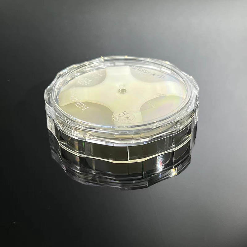
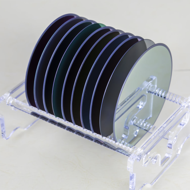
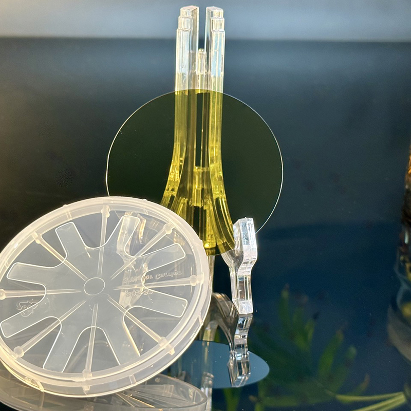
8Inch 200mm 4H-N SiC Wafer Conductive dummy research grade
8Inch 200mm 4H-N SiC Wafer Conductive dummy research grade
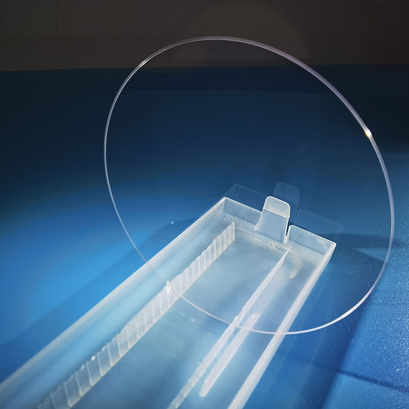
Get reliable 8-inch 200mm 4H-N SiC wafer conductive dummy of research grade from our factory. We offer high-quality products for advanced research purposes.
Due to its unique physical and electronic properties, 200mm SiC wafer semiconductor material is used to create high-performance, high-temperature, radiation-resistant, and high-frequency electronic devices. 8inch SiC substrate price is decreasing gradually as the technology becomes more advanced and the demand grows. Recent technology developments lead to production scale manufacturing of 200mm SiC wafers. The main advantages of SiC wafer semiconductor materials in comparison with Si and GaAs wafers: The electric field strength of 4H-SiC during avalanche breakdown is more than an order of magnitude higher than the corresponding values for Si and GaAs. This leads to a significant decrease in the on-state resistivity Ron. Low on-state resistivity, combined with high current density and thermal conductivity, allows the use of very small die for power devices. The high thermal conductivity of SiC reduces the thermal resistance of the chip. The electronic properties of devices based of SiC wafers are very stable over time and on temperature stable, which ensures high reliability of products. Silicon carbide is extremely resistant to hard radiation, which does not degrade the electronic properties of the chip. The high limiting operating temperature of the crystal (more than 6000C) allows you to create highly reliable devices for harsh operating conditions and special applications. At present, we can supply small batch 200mmSiC wafers steadily and continuously and have some stock in the warehouse.