| Orientation | C(0001)-Axis | R(1-102)-Axis | M(10-10) -Axis | A(11-20)-Axis | ||
| Physical property | The C axis has crystal light, and the other axes have negative light. Plane C is flat, preferably cut. | R-plane little harder than A. | M plane is stepped serrated, not easy to cut, easy to cut. | The hardness of A-plane is significantly higher than that of C-plane, which is manifested in wear resistance, scratch resistance and high hardness; Side A-plane is a zigzag plane, which is easy to cut; | ||
| Applications | C-oriented sapphire substrates are used to grow III-V and II-VI deposited films, such as gallium nitride, which can produce blue LED products, laser diodes, and infrared detector applications. This is mainly because the process of sapphire crystal growth along the C-axis is mature, the cost is relatively low, the physical and chemical properties are stable, and the technology of epitaxy on the C-plane is mature and stable. | R-oriented substrate growth of different deposited silicon extrasystals, used in microelectronics integrated circuits. In addition, high-speed integrated circuits and pressure sensors can also be formed in the process of film production of epitaxial silicon growth. R-type substrate can also be used in the production of lead, other superconducting components, high resistance resistors, gallium arsenide. | It is mainly used to grow non-polar/semi-polar GaN epitaxial films to improve the luminous efficiency. | A-oriented to the substrate produces a uniform permittivity/medium, and a high degree of insulation is used in hybrid microelectronics technology. High temperature superconductors can be produced from A-base elongated crystals. | ||
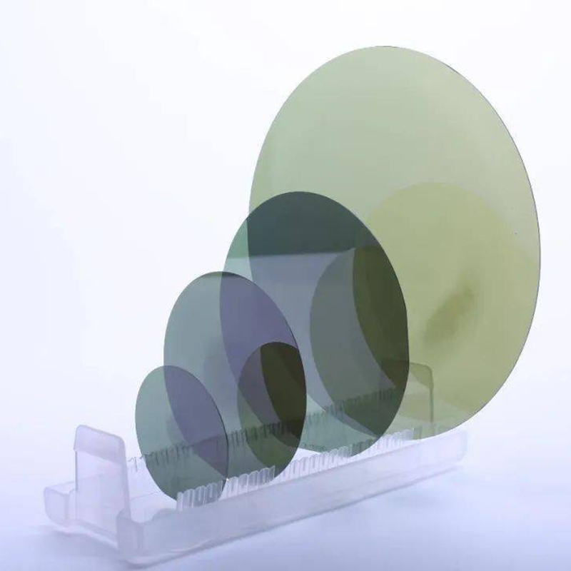
| Processing capacity | Pattern Sapphire Substrate (PSS) : In the form of Growth or Etching, nanoscale specific regular microstructure patterns are designed and made on the sapphire substrate to control the light output form of the LED, and reduce the differential defects among GaN growing on the sapphire substrate, improve the epitaxy quality, and enhance the internal quantum efficiency of the LED and increase the efficiency of light extraction. In addition, sapphire prism, mirror, lens, hole, cone and other structural parts can be customized according to customer requirements. | |||||
| Property declaration | Density | Hardness | melt point | Refractive index (visible and infrared) | Transmittance (DSP) | Dielectric constant |
| 3.98g/cm3 | 9(mohs) | 2053℃ | 1.762~1.770 | ≥85% | 11.58@300K at C axis(9.4 at A axis) | |