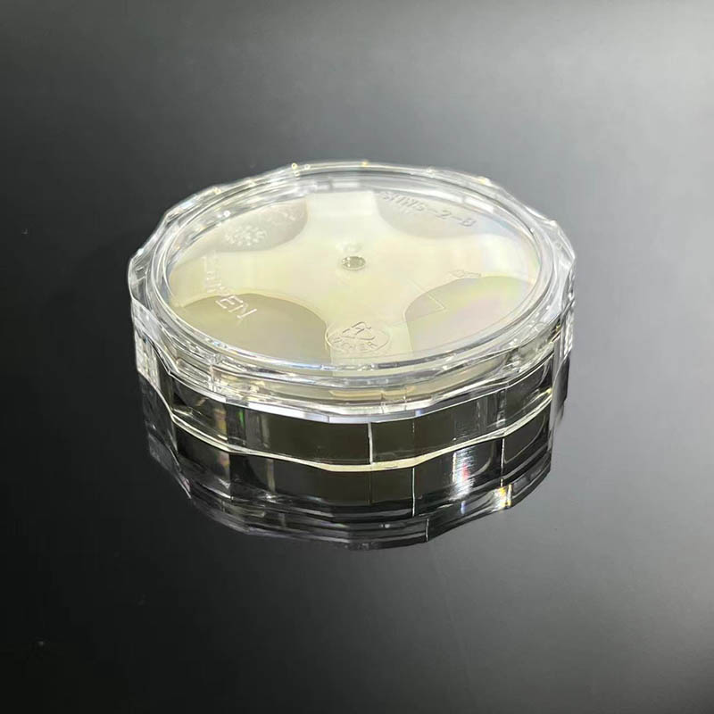
Shop high-quality 8-inch 200mm Sapphire Wafer Carrier Substrates (SSP/DSP) with thickness options of 0.5mm & 0.75mm. We are a reliable factory. Order now!
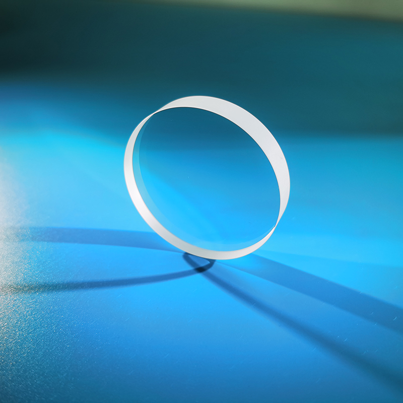
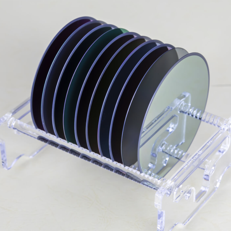
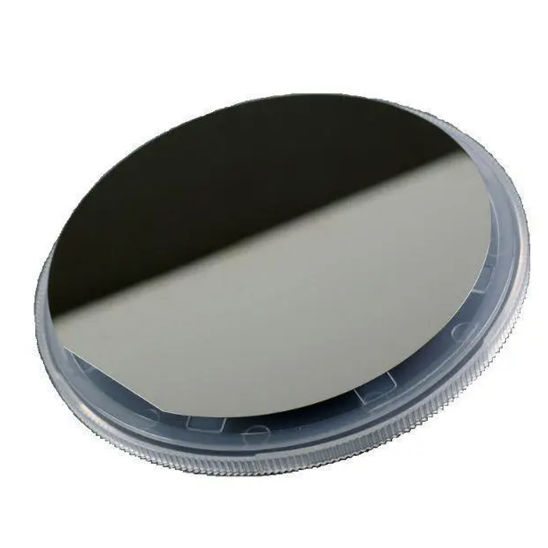
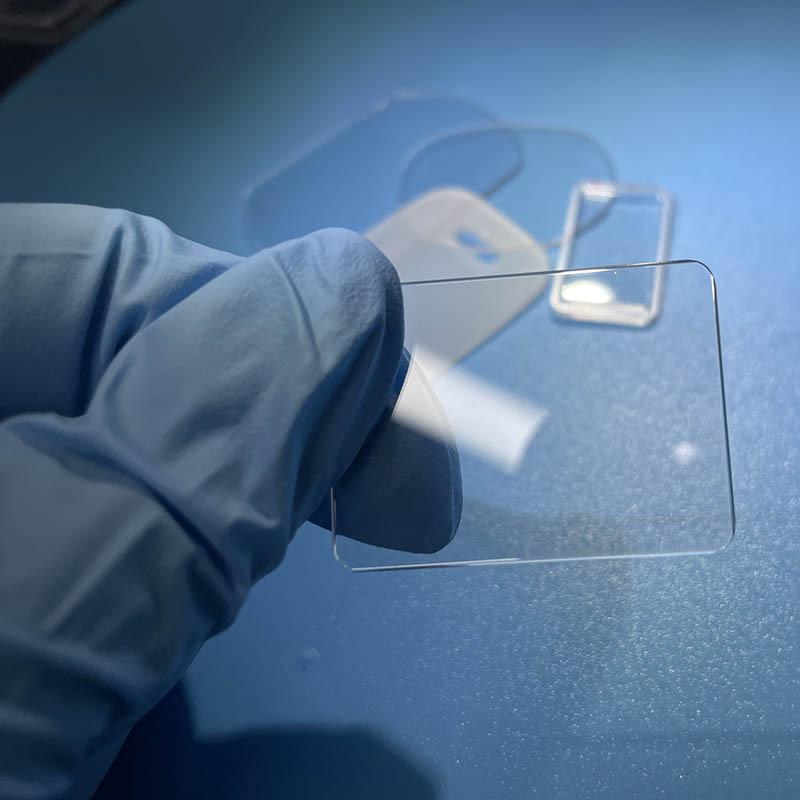
Manufacturing Method: The manufacturing process of the 8-inch sapphire substrate involves several steps. First, high-purity alumina powder is melted at ahigh temperature to form a molten state. Then, a seed crystal is immersed into the melt, allowing the sapphire to grow as the seedis slowly withdrawn. After sufficient growth, the sapphire crystal is carefully cut into thin wafers, which are then polished toachieve a smooth and flawless surface.The applications of 8-inch sapphire substrate: The 8-inch sapphire substrate is widely used in the semiconductor industry, specifically in the production of electronic devices andoptoelectronic components. It serves as a crucial foundation for the epitaxial growth of semiconductors, enabling the formation ofhigh-performance integrated circuits, light-emitting diodes (LEDs), and laser diodes. The sapphire substrate also finds applicationsin the manufacturing of optical windows, watch faces, and protective covers for smartphones and tablets- Size: The 8-inch sapphire substrate has a diameter of 200mm, providing a larger surface area for the deposition of epitaxiallayers. - Surface Quality: The surface of the substrate is carefully polished to achieve a high optical quality, with a surface roughness ofless than 0.5 nm RMS. - Thickness: The standard thickness of the substrate is 0.5 mm. However, customized thickness options are available upon request. - Packaging: The sapphire substrates are individually packaged to ensure protection during transportation and storage. They are typically placed in special trays or boxes, with appropriate cushioning materials to prevent any damage. - Edge Orientation: The substrate comes with a specified edge orientation, which is crucial for precise alignment during semiconductor manufacturing processes.In conclusion, the 8-inch sapphire substrate is a versatile and reliable material, widely used in the semiconductor industry due to its exceptional thermal, chemical, and optical properties. With its excellent surface quality and precise specifications, it serves as acrucial component in the production of high-performance electronic and optoelectronic devices.


 - Size: The 8-inch sapphire substrate has a diameter of 200mm, providing a larger surface area for the deposition of epitaxiallayers. - Surface Quality: The surface of the substrate is carefully polished to achieve a high optical quality, with a surface roughness ofless than 0.5 nm RMS. - Thickness: The standard thickness of the substrate is 0.5 mm. However, customized thickness options are available upon request. - Packaging: The sapphire substrates are individually packaged to ensure protection during transportation and storage. They are typically placed in special trays or boxes, with appropriate cushioning materials to prevent any damage. - Edge Orientation: The substrate comes with a specified edge orientation, which is crucial for precise alignment during semiconductor manufacturing processes. In conclusion, the 8-inch sapphire substrate is a versatile and reliable material, widely used in the semiconductor industry due to its exceptional thermal, chemical, and optical properties. With its excellent surface quality and precise specifications, it serves as acrucial component in the production of high-performance electronic and optoelectronic devices.