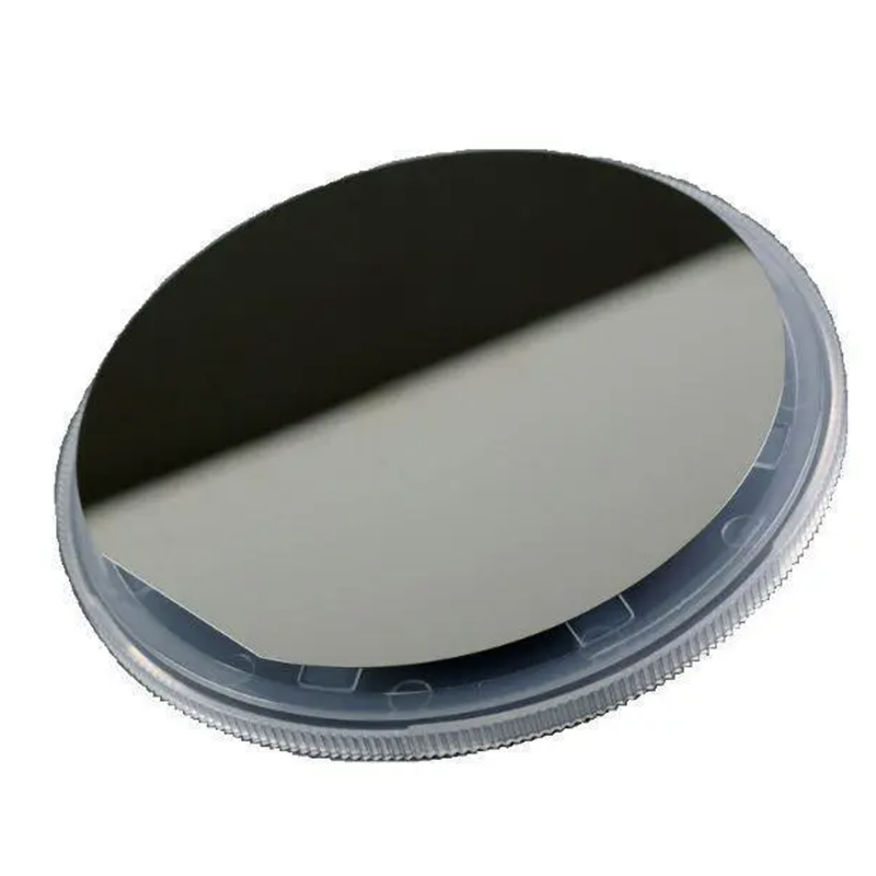
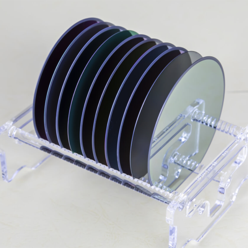
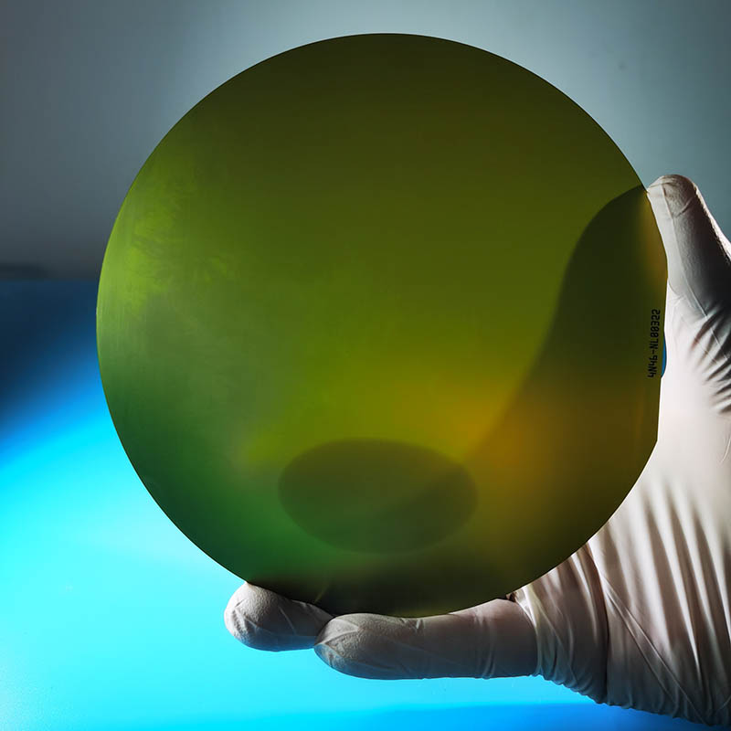
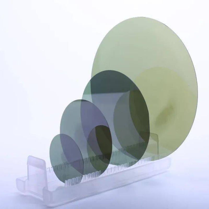
Shop our high-quality 50.8mm 2inch GaN on sapphire Epi-layer wafer products at our factory. We specialize in manufacturing and guarantee superior performance. Order now!
Based on the performance of gallium nitride, gallium nitride epitaxial chips are mainly suitable for high power, high frequency, and low voltage applications.It is reflected in:1) High bandgap: High bandgap improves the voltage level of gallium nitride devices and can output higher power than gallium arsenide devices, which is especially suitable for 5G communication base stations, military radar and other fields;2) High conversion efficiency: the on-resistance of gallium nitride switching power electronic devices is 3 orders of magnitude lower than that of silicon devices, which can significantly reduce the on-switching loss;3) High thermal conductivity: the high thermal conductivity of gallium nitride makes it have excellent heat dissipation performance, suitable for the production of high-power, high-temperature and other fields of devices;4) Breakdown electric field strength: Although the breakdown electric field strength of gallium nitride is close to that of silicon nitride, due to semiconductor process, material lattice mismatch and other factors, the voltage tolerance of gallium nitride devices is usually about 1000V, and the safe use voltage is usually below 650V.
Item
GaN-T-C-U-C50
GaN-T-C-N-C50
GaN-T-C-P-C50
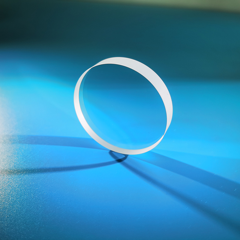
Dimensions
e 50.8mm ± 0.1mm
Thickness
4.5±0.5 um
4.5±0.5um
Orientation
C-plane(0001) ±0.5°
Conduction Type
N-type (Undoped)
N-type (Si-doped)
P-type (Mg-doped)
Resistivity(3O0K)
< 0.5 Q・cm
< 0.05 Q・cm
~ 10 Q・cm
Carrier Concentration
< 5x1017 cm-3
> 1x1018 cm-3
> 6x1016 cm-3
Mobility
~ 300 cm2/V-s
~ 200 cm2/V-s
~ 10 cm2/V-s
Dislocation Density
Less than 5x108 cm-2 (calculated by FWHMs of XRD)
Substrate structure
GaN on Sapphire(Standard: SSP Option: DSP)
Useable Surface Area
> 90%
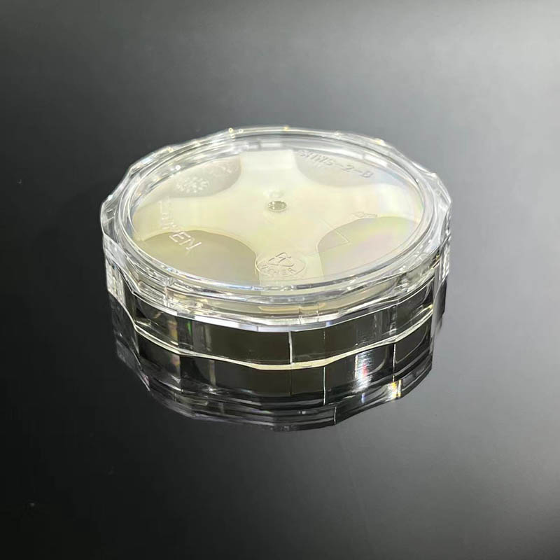
Package
Packaged in a class 100 clean room environment, in cassettes of 25pcs or single wafer containers, under a nitrogen atmosphere.