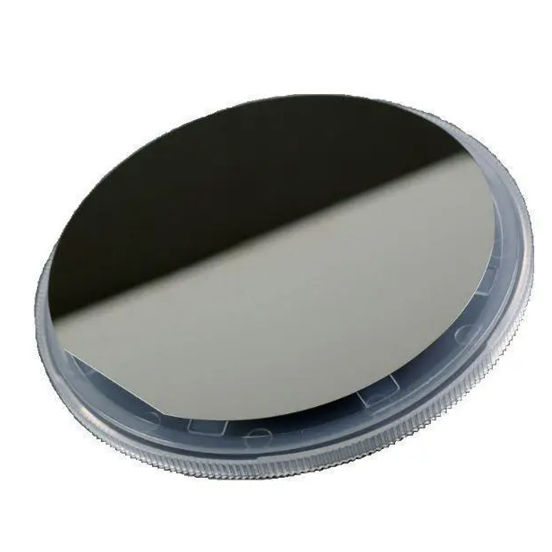
Diameter :8 inches (approximately 200mm)Thickness: Common standard thicknesses range from 0.5mm to 1mm. Other thicknesses can be customized according to specific requirementsCrystal orientation: The main common crystal orientation is 128Y-cut,Z-cut and X-cut crystal orientation, and other crystal orientation can be provided depending on the specific applicationSize Advantages: 8-inch serrata carp wafers have several size advantages over smaller wafers:Larger area: Compared to 6-inch or 4-inch wafers, 8-inch wafers provide a larger surface area and can accommodate more devices and integrated circuits, resulting in increased production efficiency and yield.Higher density: By using 8-inch wafers, more devices and components can be realized in the same area, increasing integration and device density, which in turn enhances device performance.Better consistency: Larger wafers have better consistency in the production process, helping to reduce variability in the manufacturing process and improve product reliability and consistency.The 8-inch L and LN wafers have the same diameter as mainstream silicon wafers and are easy to bond. As a high performance "jointed SAW filter" material that can handle high frequency bands.


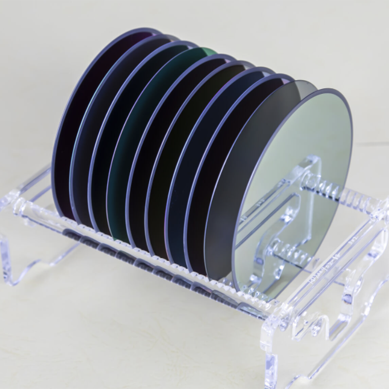
 Diameter :8 inches (approximately 200mm) Thickness: Common standard thicknesses range from 0.5mm to 1mm. Other thicknesses can be customized according to specific requirements Crystal orientation: The main common crystal orientation is 128Y-cut,Z-cut and X-cut crystal orientation, and other crystal orientation can be provided depending on the specific application Size Advantages: 8-inch serrata carp wafers have several size advantages over smaller wafers: Larger area: Compared to 6-inch or 4-inch wafers, 8-inch wafers provide a larger surface area and can accommodate more devices and integrated circuits, resulting in increased production efficiency and yield. Higher density: By using 8-inch wafers, more devices and components can be realized in the same area, increasing integration and device density, which in turn enhances device performance. Better consistency: Larger wafers have better consistency in the production process, helping to reduce variability in the manufacturing process and improve product reliability and consistency. The 8-inch L and LN wafers have the same diameter as mainstream silicon wafers and are easy to bond. As a high performance "jointed SAW filter" material that can handle high frequency bands.