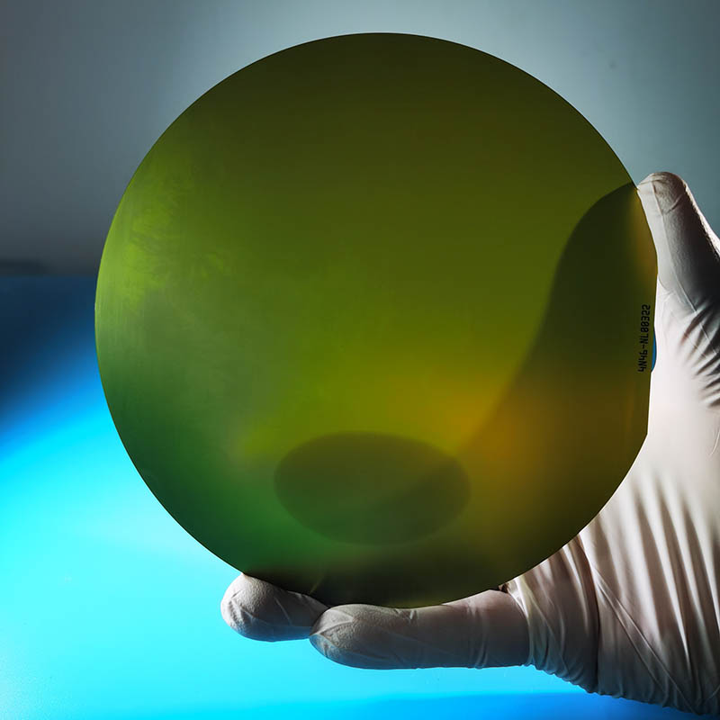
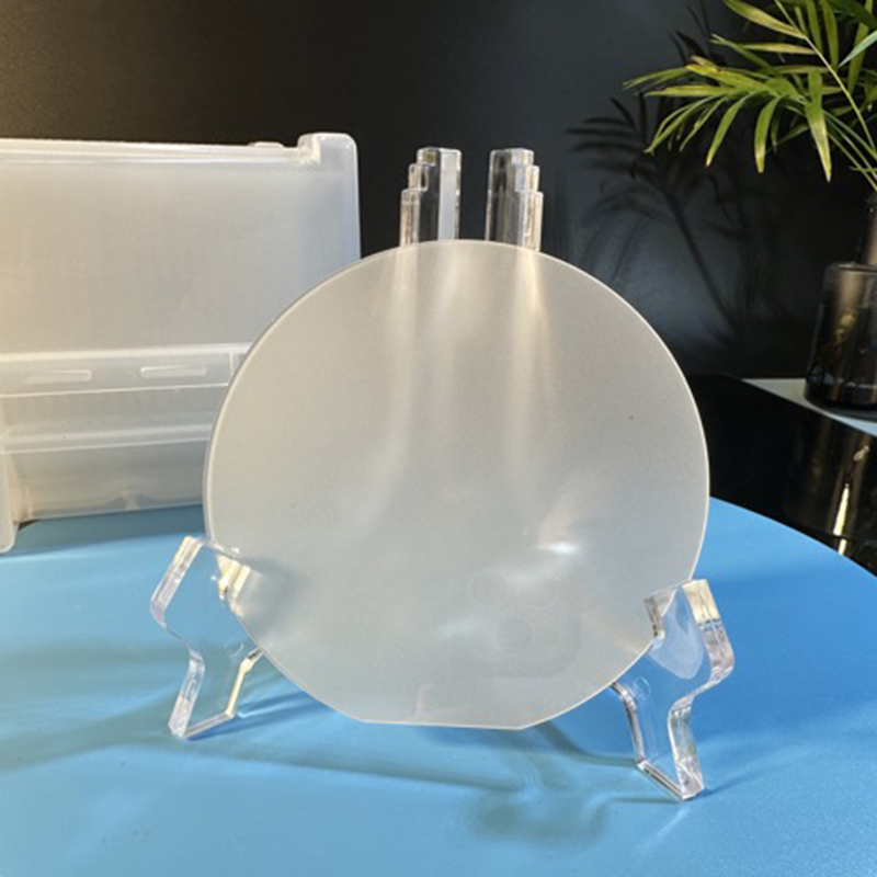
12 inch Dia300x1.0mmt Sapphire Wafer Substrate C-Plane SSP/DSP
12 inch Dia300x1.0mmt Sapphire Wafer Substrate C-Plane SSP/DSP
Shop the best quality 12 inch Dia300x1.0mmt Sapphire Wafer Substrate C-Plane SSP/DSP at our factory. We specialize in producing high-grade products for various applications.
At present, sapphire has two main uses, one is the substrate material, which is mainly LED substrate material, the other is the watch dial, aviation, aerospace, special manufacturing window material.Although silicon carbide, silicon and gallium nitride are also available as substrates for leds in addition to sapphire, mass production is still not possible due to cost and some unresolved technical bottlenecks. Sapphire substrate through the technical development in recent years, its lattice matching, electrical conductivity, mechanical properties, thermal conductivity and other properties have been greatly improved and promoted, cost-effective advantage is significant, so sapphire has become the most mature and stable substrate material in the LED industry, has been widely used in the market, the market share as high as 90%.
Orientation
C-plane<0001> +/- 1 deg.
Diameter
300.0 +/-0.25 mm
Thickness
1.0 +/-25um
Notch
Notch or Flat
TTV
<50um
BOW
<50um
Edges
Protactive chamfer
Front side – polished 80/50
Laser mark
None
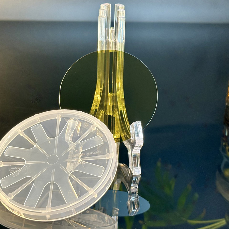
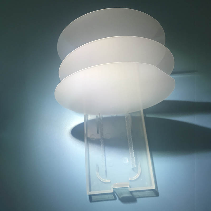
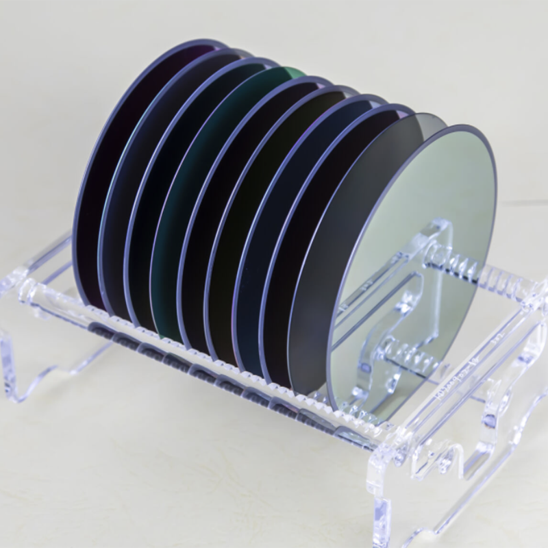
Packaging
Single wafer carrier box
Front side Epi ready polished (Ra <0,3nm)
Back side Epi ready polished (Ra <0,3nm)
1. Sapphire substrate surfaces have an extremely low particle count, with fewer than 50 particles 0.3 microns or larger per 2 inches in the 2 to 8 inch size range, and major metals (K, Ti, Cr, Mn, Fe, Co, Ni, Cu, Zn) below 2E10/cm2. The 12-inch base material is also expected to achieve this grade.2. Can be used as a carrier wafer for the 12-inch semiconductor manufacturing process (in-device transport pallets) and as a substrate for bonding.3. Can control the shape of concave and convex surface.Material: High purity single crystal Al2O3, sapphire wafer.LED quality, no bubbles, cracks, twins, lineage, no color..etc.


 1. Sapphire substrate surfaces have an extremely low particle count, with fewer than 50 particles 0.3 microns or larger per 2 inches in the 2 to 8 inch size range, and major metals (K, Ti, Cr, Mn, Fe, Co, Ni, Cu, Zn) below 2E10/cm2. The 12-inch base material is also expected to achieve this grade. 2. Can be used as a carrier wafer for the 12-inch semiconductor manufacturing process (in-device transport pallets) and as a substrate for bonding. 3. Can control the shape of concave and convex surface. Material: High purity single crystal Al2O3, sapphire wafer. LED quality, no bubbles, cracks, twins, lineage, no color..etc.