● Growth substrate for III-V and II-VI compounds.● Electronics and optoelectronics.● IR applications.● Silicon On Sapphire Integrated Circuit(SOS).● Radio Frequency Integrated Circuit(RFIC).In LED production, sapphire wafers are used as a substrate for the growth of gallium nitride (GaN) crystals, which emit light when an electric current is applied. Sapphire is an ideal substrate material for GaN growth because it has a similar crystal structure and thermal expansion coefficient to GaN, which minimizes defects and improves crystal quality.In optics, sapphire wafers are used as windows and lenses in high-pressure and high-temperature environments, as well as in infrared imaging systems, because of their high transparency and hardness.
Item
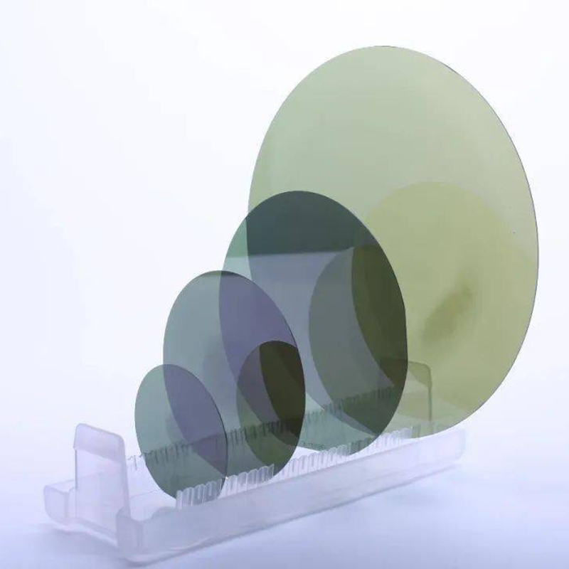
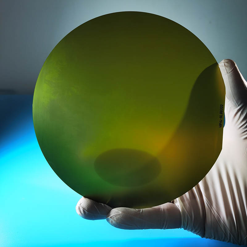
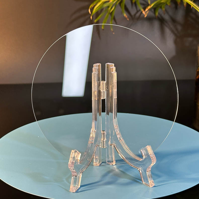
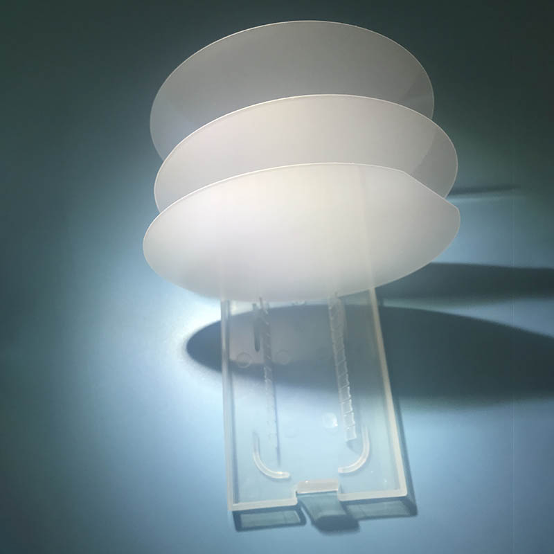
4-inch C-plane(0001) 650μm Sapphire Wafers
Crystal Materials
99,999%, High Purity, Monocrystalline Al2O3
Grade
Prime, Epi-Ready
Surface Orientation
C-plane(0001)
C-plane off-angle toward M-axis 0.2 +/- 0.1°
Diameter
100.0 mm +/- 0.1 mm
Thickness
650 μm +/- 25 μm
Primary Flat Orientation
A-plane(11-20) +/- 0.2°
Primary Flat Length
30.0 mm +/- 1.0 mm
Single Side Polished
Front Surface
Epi-polished, Ra < 0.2 nm (by AFM)
(SSP)
Back Surface
Fine ground, Ra = 0.8 μm to 1.2 μm
Double Side Polished
Front Surface
Epi-polished, Ra < 0.2 nm (by AFM)
(DSP)
Back Surface
Epi-polished, Ra < 0.2 nm (by AFM)
TTV
< 20 μm
BOW
< 20 μm
WARP
< 20 μm
Cleaning / Packaging
Class 100 cleanroom cleaning and vacuum packaging,
25 pieces in one cassette packaging or single piece packaging.
Generally speaking, we provide the package by 25pcs cassette box; we also can packed by single wafer container under 100 grade cleaning room according to the client's requirement.


 Generally speaking, we provide the package by 25pcs cassette box; we also can packed by single wafer container under 100 grade cleaning room according to the client's requirement.