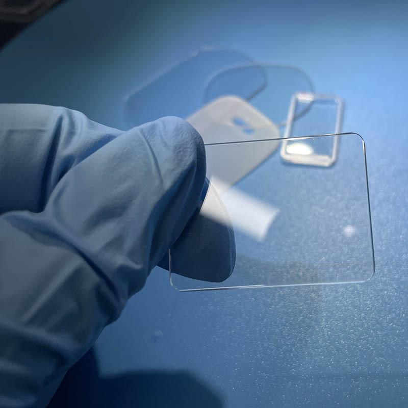
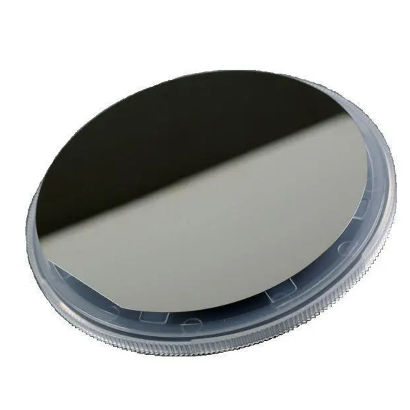
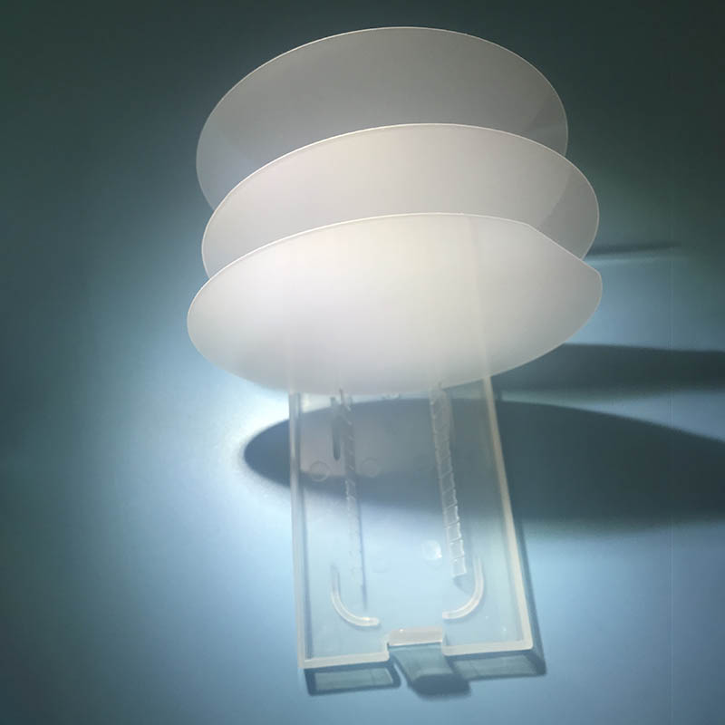
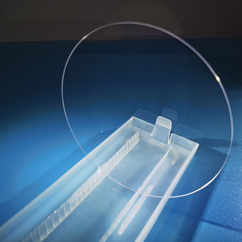
100mm 4inch GaN on Sapphire Epi-layer wafer Gallium nitride epitaxial wafer
100mm 4inch GaN on Sapphire Epi-layer wafer Gallium nitride epitaxial wafer
Shop the highest quality GaN on Sapphire Epi-layer wafers at our factory. We specialize in producing 100mm 4inch Gallium nitride epitaxial wafers for a variety of applications.
(1) High temperature baking, sapphire substrate is first heated to 1050℃ in a hydrogen atmosphere, the purpose is to clean the substrate surface;(2) When the substrate temperature drops to 510℃, a low-temperature GaN/AlN buffer layer with a thickness of 30nm is deposited on the surface of the sapphire substrate;(3) Temperature rise to 10 ℃, the reaction gas ammonia, trimethylgallium and silane are injected, respectively control the corresponding flow rate, and the silicon-doped N-type GaN of 4um thickness is grown;(4) The reaction gas of trimethyl aluminum and trimethyl gallium was used to prepare silicon-doped N-type A⒑ continents with a thickness of 0.15um;(5) 50nm Zn-doped InGaN was prepared by injecting trimethylgallium, trimethylindium, diethylzinc and ammonia at a temperature of 8O0℃ and controlling different flow rates respectively;(6) The temperature was increased to 1020℃, trimethylaluminum, trimethylgallium and bis (cyclopentadienyl) magnesium were injected to prepare 0.15um Mg doped P-type AlGaN and 0.5um Mg doped P-type G blood glucose;(7) High quality P-type GaN Sibuyan film was obtained by annealing in nitrogen atmosphere at 700℃;(8) Etching on the P-type G stasis surface to reveal the N-type G stasis surface;(9) Evaporation of Ni/Au contact plates on p-GaNI surface, evaporation of △/Al contact plates on ll-GaN surface to form electrodes.
Item
GaN-T-C-U-C100
GaN-T-C-N-C100
Dimensions
e 100 mm ± 0.1 mm
Thickness
4.5±0.5 um Can be customized
Orientation
C-plane(0001) ±0.5°
Conduction Type
N-type (Undoped)
N-type (Si-doped)
Resistivity(300K)
< 0.5 Q・cm
< 0.05 Q・cm
Carrier Concentration
< 5x1017 cm-3
> 1x1018 cm-3
Mobility
~ 300 cm2/V-s
~ 200 cm2/V-s
Dislocation Density
Less than 5x108 cm-2 (calculated by FWHMs of XRD)
Substrate structure
GaN on Sapphire(Standard: SSP Option: DSP)
Useable Surface Area
> 90%
Package
Packaged in a class 100 clean room environment, in cassettes of 25pcs or single wafer containers, under a nitrogen atmosphere.