2inch 50.8mm Germanium Wafer Substrate Single crystal 1SP 2SP

Get high-quality Germanium Wafer Substrate for your industry needs. Our factory produces 2inch (50.8mm) single crystal 1SP and 2SP wafers. Order now!

Request a Quote
  • 2inch 50.8mm Germanium Wafer Substrate Single crystal 1SP 2SP
  • 2inch 50.8mm Germanium Wafer Substrate Single crystal 1SP 2SP
  • 2inch 50.8mm Germanium Wafer Substrate Single crystal 1SP 2SP

PRODUCTS DETAILS

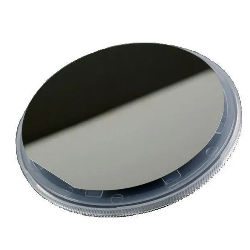
Germanium chips have semiconductor properties. Has played an important role in the development of solid state physics and solid state electronics. Germanium has a melting density of 5.32g/cm 3, germanium may be classified as a thin scattered metal, germanium chemical stability, does not interact with air or water vapor at room temperature, but at 600 ~ 700℃, germanium dioxide is quickly generated. Does not work with hydrochloric acid, dilute sulfuric acid. When concentrated sulfuric acid is heated, germanium will slowly dissolve. In nitric acid and aqua regia, germanium is easily dissolved. The effect of alkali solution on germanium is very weak, but molten alkali in air can make germanium dissolve quickly. Germanium does not work with carbon, so it is melted in a graphite crucible and will not be contaminated by carbon. Germanium has good semiconductor properties, such as electron mobility, hole mobility and so on. The development of germanium still has great potential.
Growth method CZ
crystal instuture Cubic system
Lattice constant a=5.65754 Å       
Density 5.323g/cm3
Melting point 937.4℃
Doping Un-doping Doping-Sb Doping-Ga
Type /

N

P
resistence >35Ωcm 0.01~35 Ωcm 0.05~35 Ωcm
EPD <4×10³∕cm2 <4×10³∕cm2 <4×10³∕cm2
Diameter 2inch/50.8 mm
Thickness 0.5mm,1.0mm
Surface DSP and SSP
Orientation <100>、<110>、<111>、±0.5º
Ra ≤5Å(5µm×5µm)
Package 100 grade package ,1000 grade room

Hot Products

200mm 8inch GaN on sapphire Epi-layer wafer substrate

200mm 8inch GaN on sapphire Epi-layer wafer substrate

8 inch 200mm Sapphire Wafer Carrier Subsrate SSP DSP Thickness 0.5mm 0.75mm

8 inch 200mm Sapphire Wafer Carrier Subsrate SSP DSP Thickness 0.5mm 0.75mm

8 Inch Lithium Niobate Wafer LiNbO3 LN wafer

8 Inch Lithium Niobate Wafer LiNbO3 LN wafer

2 inch Silicon Carbide Wafers 6H or 4H N-type or Semi-Insulating SiC Substrates

2 inch Silicon Carbide Wafers 6H or 4H N-type or Semi-Insulating SiC Substrates

High precision Dia50x5mmt Sapphire Windows High temperature resistance and high hardness

High precision Dia50x5mmt Sapphire Windows High temperature resistance and high hardness

150mm 200mm 6inch 8inch  GaN on Silicon Epi-layer wafer Gallium nitride epitaxial wafer

150mm 200mm 6inch 8inch GaN on Silicon Epi-layer wafer Gallium nitride epitaxial wafer

50.8mm 2inch GaN on sapphire Epi-layer wafer

50.8mm 2inch GaN on sapphire Epi-layer wafer

8Inch 200mm 4H-N SiC Wafer Conductive dummy research grade

8Inch 200mm 4H-N SiC Wafer Conductive dummy research grade

Dia50.8mm Sapphire Wafer Sapphire Window High Optical Transmittance DSP/SSP

Dia50.8mm Sapphire Wafer Sapphire Window High Optical Transmittance DSP/SSP

Sapphire window optical elements coated multi-size specifications Optical infrared window

Sapphire window optical elements coated multi-size specifications Optical infrared window

Contact us

Please feel free to give your inquiry in the form below We will reply you in 24 hours