Features of single crystal sapphire1. Sapphire has a high optical transmittance, so it is widely used as microelectronic tube dielectric material, ultrasonic conduction element, waveguide laser cavity, and other optical elements, as window materials for infrared military devices, space vehicles, high-intensity lasers and optical communications.2. Sapphire has high rigidity, high strength, high working temperature, abrasion resistance, corrosion resistance characteristics, so sapphire substrate is often used in harsh environments, such as boiler water gauge (high-temperature resistance), commodity bar code scanner, bearing, and other precision manufacturing (wear resistance), coal, gas, well detection sensors and detector windows (anti-corrosion).3. Sapphire has the characteristics of electrical insulation, transparency, good thermal conductivity, and high rigidity, so it can be used as the substrate material of integrated circuits, such as LED and microelectronic circuits, ultra-high-speed integrated circuit.
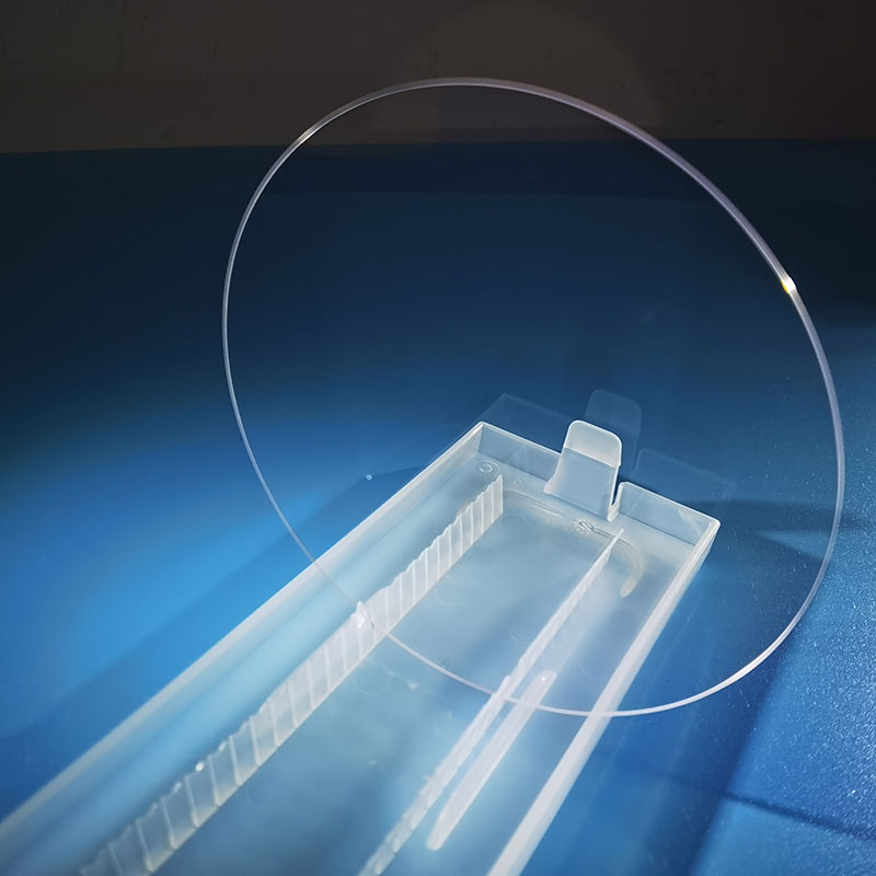
Diameter
50.8mm +/-0.1mm or +/-0.02mm
Thickness
0.43mm± 0.1mm or +/-0.02mm
Orientation
C-plane/A-Plane/M-Plane/R-Plane
Surface quality (scratch & dig)
60/40, 40/20 or better
Surface accuracy
λ/10, λ/2, λ
Clear Aperture
>85%, >90%
Parallelism
+/-3', +/-30''
Bevel
0.1~0.3mm×45 degree
Coating
AR, BBAR or upon customer request( UV, VIS, IR)
What is your minimum order requirement?MOQ: 25 piece.How long will it take to execute my order and delivery it?Confirm the order 1days After confirming the payment and delivery in 5days if on stocks.Can you give warranty of your products?We promise the quality, if the quality has any problems, we will produce new produces or return you money.How to pay? T/T, Paypal, West Union, bank transfer.HOW about the freight?We can help you pay for the fee if you don't have account, if the order is over 10000usd, we can delivery by CIF.If you have any other questions, please do not hesitate to contact me.Connect with by skype/whatsapp: +86 158 0194 2596 or[email protected]We are at your side any time!
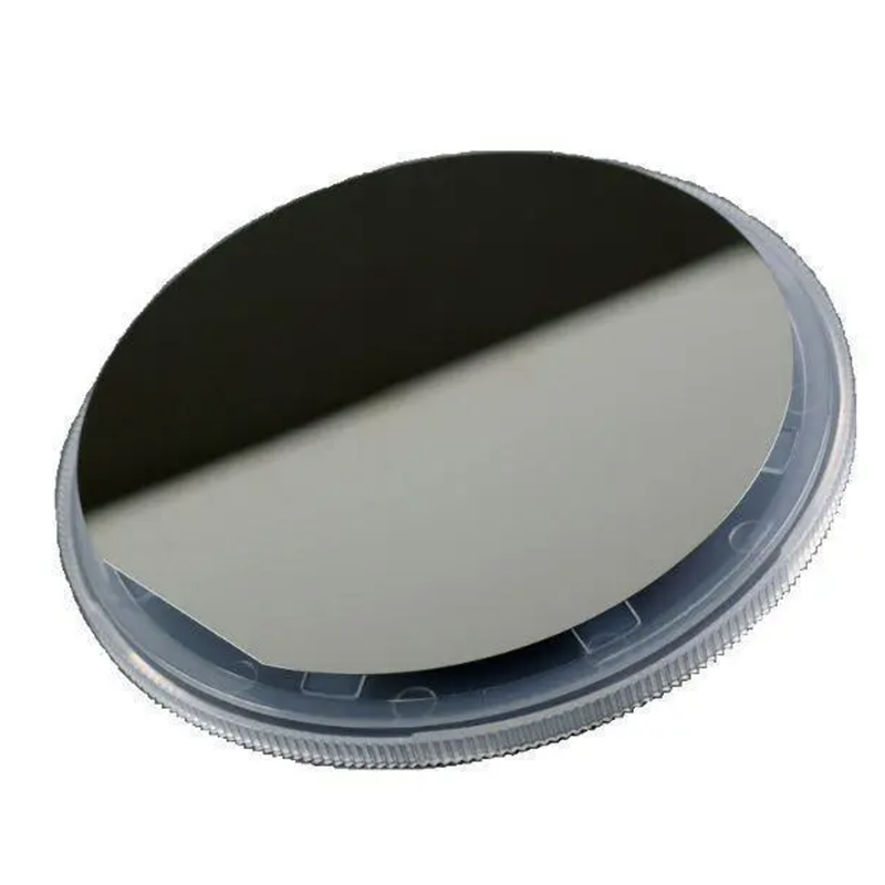
No
Properties
Target
Tolerance
Remarks
1
Diameter
50.8mm
± 0.1mm
2
Thickness
430μm
±15μm
3
Surface orientation of C-plane
off C-axis to M0.2°
± 0.1°
4
Primary flat length
16mm
±11mm
5
Primary flat orientation
A-plane(11-20)
±0.1°
6
Back side Roughness
0.8~1.2um
7
Front side Roughness
<0.3nm
8
Wafer edge
R-type
9
Total Thickness Variation, TTV
≤ 10μm(LTV≤5μm, 5*5)
10
SORI
≤10μm
11
Bow
-10 μm ≤ BOW ≤ 0
12
Laser Mark
N/A
not have
Package
25 wafers in one cassette
Trace ability
Wafers shall be traceable with respect to cassette number