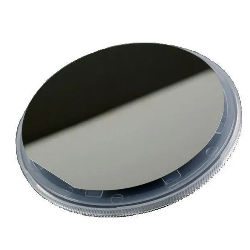
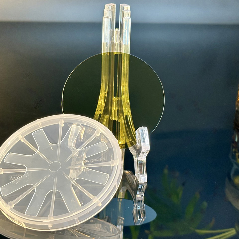
4H-N 4 inch SiC substrate wafer Silicon Carbide Production Dummy Research grade
4H-N 4 inch SiC substrate wafer Silicon Carbide Production Dummy Research grade
Discover our 4H-N 4-inch SiC substrate wafer, ideal for silicon carbide production. As a factory, we specialize in high-quality research-grade products.
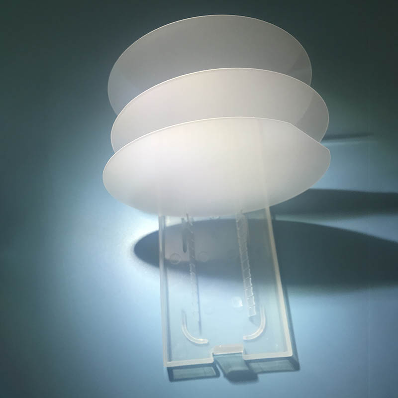
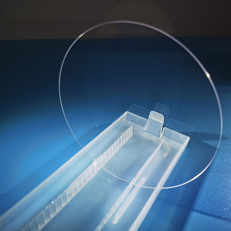
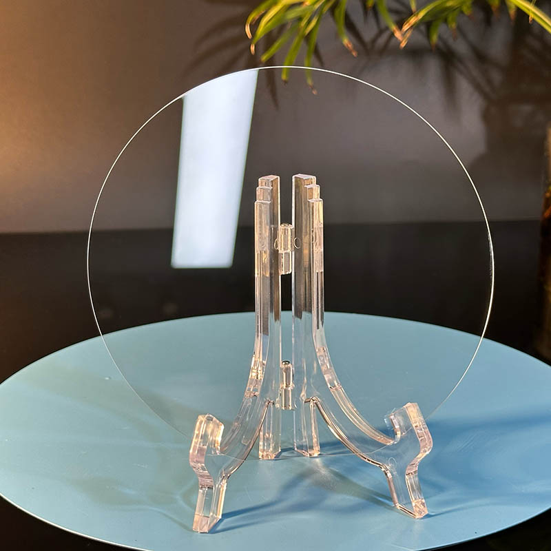
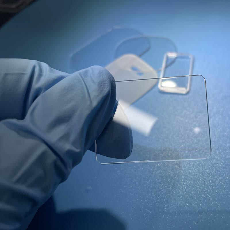
4-inch silicon carbide single crystal substrate wafers play an important role in many fields. First, it is widely used in the semiconductor industry in the preparation of high-power electronic devices such as power transistors, integrated circuits and power modules. Its high thermal conductivity and high temperature resistance enable it to dissipate heat better and provide greater working efficiency and reliability. Secondly, silicon carbide wafers are also used in the research field to carry out research on new materials and devices. In addition, silicon carbide wafers are also widely used in optoelectronics, such as the manufacture of leds and laser diodes.4-inch silicon carbide single crystal substrate wafer diameter of 4 inches (about 101.6mm), surface finish up to Ra < 0.5 nm, thickness of 600±25 μm. The conductivity of the wafer is N type or P type and can be customized according to customer needs. In addition, the chip also has excellent mechanical stability, can withstand a certain amount of pressure and vibration.inch silicon carbide single crystal substrate wafer is a high-performance material widely used in semiconductor, research and optoelectronics fields. It has excellent thermal conductivity, mechanical stability and high temperature resistance, which is suitable for the preparation of high power electronic devices and the research of new materials. We offer a variety of specifications and customization options to meet a variety of customer needs. Please pay attention to our independent site to learn more about the product information of silicon carbide wafers.Key works: Silicon carbide wafers, silicon carbide single crystal substrate wafers, 4 inches, thermal conductivity, mechanical stability, high temperature resistance, power transistors, integrated circuits, power modules, leds, laser diodes, surface finish, conductivity, custom options


 4-inch silicon carbide single crystal substrate wafer diameter of 4 inches (about 101.6mm), surface finish up to Ra < 0.5 nm, thickness of 600±25 μm. The conductivity of the wafer is N type or P type and can be customized according to customer needs. In addition, the chip also has excellent mechanical stability, can withstand a certain amount of pressure and vibration. inch silicon carbide single crystal substrate wafer is a high-performance material widely used in semiconductor, research and optoelectronics fields. It has excellent thermal conductivity, mechanical stability and high temperature resistance, which is suitable for the preparation of high power electronic devices and the research of new materials. We offer a variety of specifications and customization options to meet a variety of customer needs. Please pay attention to our independent site to learn more about the product information of silicon carbide wafers. Key works: Silicon carbide wafers, silicon carbide single crystal substrate wafers, 4 inches, thermal conductivity, mechanical stability, high temperature resistance, power transistors, integrated circuits, power modules, leds, laser diodes, surface finish, conductivity, custom options