
- Home
- Blog
- Advancement in Semiconductor Manufacturing: New 8 Inch Wafer Diameter Promises Enhanced Efficiency
Advancement in Semiconductor Manufacturing: New 8 Inch Wafer Diameter Promises Enhanced Efficiency
By:Admin
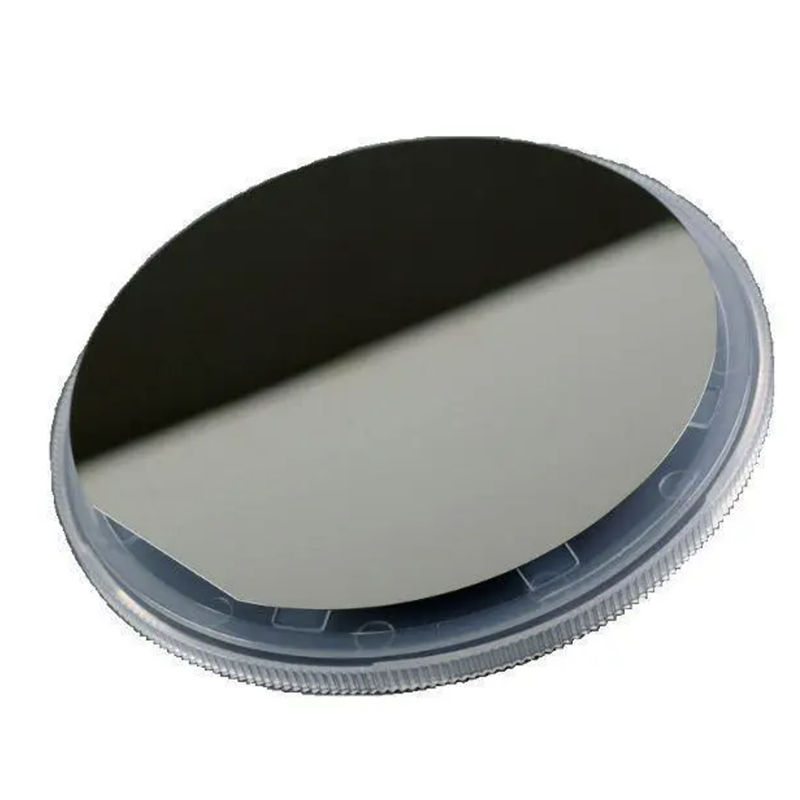
[City], [Date] - [Company Name], a leading provider of innovative semiconductor solutions, has unveiled its latest breakthrough in semiconductor manufacturing with the introduction of an advanced 8-inch wafer diameter. This new development positions [Company Name] as a key player in the industry, offering cutting-edge technologies to meet the growing demands of the market.
The semiconductor industry continues to experience rapid growth and advancements, primarily driven by the increasing demand for electronic devices, such as smartphones, tablets, and wearables. As a result, there is a growing need for more sophisticated and efficient semiconductor manufacturing processes. [Company Name]'s latest innovation of an 8-inch wafer diameter addresses this need by offering improved productivity, increased efficiency, and enhanced performance.
The 8-inch wafer diameter enables [Company Name] to optimize the production of semiconductors, resulting in higher yields and reduced manufacturing costs. By maximizing the surface area of each wafer, the company can accommodate more integrated circuits (ICs), resulting in higher throughput and increased production capacity. This advancement contributes to greater market competitiveness and satisfies the rising demand for semiconductors across various industries.
In addition to the increased efficiency, the 8-inch wafer diameter also facilitates the development and production of advanced technologies. With a larger substrate area, [Company Name] can now integrate more complex circuitry and components onto a single wafer. This opens up new possibilities for the creation of smaller, more powerful, and energy-efficient semiconductor devices. Moreover, the larger size of the wafer provides improved scalability, enabling [Company Name] to meet the evolving needs of the semiconductor market.
[Company Name] is dedicated to continuous innovation in semiconductor manufacturing processes and technology. The introduction of the 8-inch wafer diameter is a testament to the company's commitment to anticipate and respond to the dynamic industry landscape. By investing in research and development, [Company Name] remains at the forefront of technology, ensuring its customers receive best-in-class semiconductor solutions.
"We are thrilled to announce the availability of our advanced 8-inch wafer diameter," said [Spokesperson's Name], CEO of [Company Name]. "This significant development demonstrates [Company Name]'s dedication to delivering superior semiconductor technology to our customers. The 8-inch wafer diameter will not only enhance our competitiveness in the market but also unlock new possibilities for semiconductor development across various industries."
Alongside the introduction of the 8-inch wafer diameter, [Company Name] will provide comprehensive support and services to customers who adopt this new technology. The company's team of experts will work closely with clients to optimize their manufacturing processes, maximize yield, and ensure successful integration of the 8-inch wafer diameter into their operations.
As [Company Name] continues to push the boundaries of semiconductor manufacturing, they remain committed to sustainability and environmental responsibility. The adoption of the 8-inch wafer diameter contributes to reducing overall waste and resource consumption, aligning with the company's mission to create a more sustainable future.
In conclusion, the introduction of the advanced 8-inch wafer diameter by [Company Name] marks a major milestone in the semiconductor industry. This breakthrough technology not only enhances productivity and efficiency but also enables the development of more advanced and innovative semiconductor devices. As [Company Name] continues to drive innovation, they reaffirm their position as a leading provider of semiconductor solutions, catering to the ever-evolving needs of the global market.
Company News & Blog
The surprising science behind quartz crystals and how they're changing technology
Innovation is at the heart of many successful companies and this is certainly true for Quartz crystal. Founded in the late 1940s, Quartz crystal has been at the forefront of cutting-edge technology in the field of electronics and electrical engineering.Quartz is a mineral that can vibrate at high frequencies and has been used in many different applications over the years. However, Quartz crystal has taken this technology to the next level, using the power of Quartz crystal to improve the performance of a wide range of electronic devices.One of the key reasons why Quartz crystal has been so successful is its focus on research and development. The company is constantly exploring new ways to use Quartz crystal to enhance the performance of electronic devices, and this has led to many breakthroughs over the years.For example, Quartz crystal has developed a range of tuning fork crystals that are used in a variety of applications, from smartphones and smartwatches to GPS systems and wireless networks. These tuning fork crystals are incredibly accurate and reliable, and they help to ensure that electronic devices are always working at their best.Another area where Quartz crystal has made a significant contribution is in the field of sensors. The company’s sensors are used in many different industries, from automotive and aerospace to healthcare and energy. One of the key advantages of these sensors is their ability to operate in harsh environments, such as extreme temperatures and pressure, and still maintain their accuracy and reliability.Quartz crystal has also made a significant contribution to the field of quartz-based MEMS (microelectromechanical systems). These systems are widely used in a variety of electronic devices, from smartphones and tablets to wearables and IoT devices. Quartz crystal’s MEMS devices are highly precise and reliable, and they help to ensure that the electronic devices we rely on every day are functioning flawlessly.Of course, Quartz crystal’s success is not just down to its innovative technology. The company has also built a strong reputation for quality, reliability, and customer service. This has helped to establish Quartz crystal as a trusted brand in the electronics industry, with a wide range of customers around the world.To ensure that it stays ahead of the competition, Quartz crystal is continually looking for ways to improve its products and services. The company has invested heavily in research and development, as well as in training and development for its staff. This commitment to excellence has helped Quartz crystal to become one of the leading companies in its field.Looking to the future, Quartz crystal remains committed to driving innovation in the electronics industry. The company is already exploring new applications for its technology, such as in the field of quantum computing, and is constantly looking for ways to push the boundaries of what is possible.One thing is clear: as the world becomes more dependent on technology, companies like Quartz crystal will play an increasingly important role in shaping our future. Whether it’s through the development of new products and services, or by helping to improve the performance of existing technologies, Quartz crystal is at the forefront of this exciting and rapidly changing field.
Breakthrough in Crystalline Material: SrTiO3 Wafer Holds Potential for Revolutionary Applications
A new technology using SrTiO3 wafers promises to revolutionize the semiconductor industry by improving the efficiency and performance of electronic devices. SrTiO3 is a unique material with exceptional electrical and optical properties that make it ideal for use in electronic devices such as computers, smartphones, and other digital devices.SrTiO3 is a complex oxide compound made up of Strontium, Titanium, and Oxygen. It exhibits semiconducting properties, which is why it’s relevant to the electronics industry. The technology is particularly useful in the development of advanced semiconductor devices such as MOSFETs, solar cells, and transistors, among others.SrTiO3 wafers have been in use in the semiconductor industry for years, but scientists have been exploring ways to make the compound material more efficient and precise. New research shows that combining SrTiO3 with other materials, such as hafnium oxide, can produce even more remarkable results.The company behind this breakthrough development is a leading producer of high-quality wafers for the electronics industry. The company has been a pioneer in the development of semiconductor-grade crystals, and its technological advancements continue to push the boundaries of what is possible within the industry.The SrTiO3 wafer technology has significant implications for the future of the electronics industry. Manufacturers can use the technology to develop devices that are more powerful, efficient, and affordable. The use of SrTiO3 wafers in the manufacturing process ensures that electronic components are more reliable and can operate at higher temperatures.The technology also has significant benefits for solar cell technology. SrTiO3-based solar cells have higher conversion efficiencies than conventional cells, making them more desirable for use in photovoltaic systems. The use of this technology in solar panels could lead to the development of more efficient and cost-effective solar panels, helping bring clean energy to millions of people worldwide.The innovative SrTiO3 wafer technology has many applications, including in the automotive, healthcare, and aerospace industries. Researchers are exploring new uses for the technology and hope to discover new applications that will further revolutionize the electronics industry in the coming years.The company's patented manufacturing process for SrTiO3 wafers ensures the production of high-quality materials that meet strict industry standards. The company's wafers are currently being used in research and development laboratories around the world, and several companies have already adopted the technology in their manufacturing processes.The use of SrTiO3 wafers in electronic devices is set to increase in the coming years as the technology becomes more widespread and affordable. The introduction of this technology has significant implications for the electronics industry, and researchers are excited by its potential to transform the industry's future.In conclusion, the emergence of SrTiO3 wafers has set the semiconductor industry on a path towards a new generation of electronic devices. The technology has significant implications for the development of powerful, efficient, and affordable electronic devices, solar cell technology, and many other applications. With continued research and development, the technology has the potential to revolutionize the electronics industry for years to come.
Exploring the Advantages of Silicon on Sapphire Technology in Cutting-Edge Innovations
Silicon-On-Sapphire (SOS), a revolutionary technology used in making semiconductors, has emerged as a promising solution for high-frequency wireless communication and high-speed digital circuits. SOS is an advanced technology used in manufacturing electronic devices that are faster, more reliable, and efficient than traditional silicon-based technologies. This technology is highly sought after by manufacturers worldwide, and one company is leading the way in bringing it to the forefront – Skyworks Solutions.Skyworks Solutions, Inc. (need remove brand name) is a company that is committed to making cutting-edge products that help connect people around the world. One of their main products is radio frequency integrated circuits (RFICs), which are critical components in wireless communication devices, including smartphones, tablets, and IoT devices. For over 20 years, Skyworks has been at the forefront of RFIC production, and now they are leveraging the power of SOS to take their products to the next level.What is Silicon-On-Sapphire?Before we delve into some of the amazing things that Skyworks is doing with SOS technology, let's first take a moment to understand what SOS is. SOS is a type of material used in the production of semiconductors. The material is essentially a layer of silicon deposited on top of a substrate of sapphire. The combination of these two materials creates a stable and durable platform on which to build electronic devices.SOS has several advantages over traditional silicon-based technologies. For one, it has a higher electron mobility, which means that electrons can move more quickly and with less resistance. This increased electron mobility makes SOS ideal for high-frequency wireless communication and high-speed digital circuits, both of which require fast and reliable data transmission.Another advantage of SOS is that it has a higher breakdown voltage than silicon. This means that it can handle higher voltages without becoming damaged. This makes SOS ideal for use in high-power applications.Skyworks Solutions: Using SOS to Create Cutting-Edge ProductsNow that we've covered the basics of SOS, let's take a look at what Skyworks is doing with this technology. Skyworks has long been a leader in producing RFICs that are used in wireless communication devices. However, with the increasing demand for faster and more reliable data transmission, Skyworks saw an opportunity to leverage the power of SOS to create even better products.One area in which Skyworks is using SOS is in the production of 5G wireless communication devices. 5G is the next generation of wireless communication technology, and it promises to be faster and more reliable than current 4G networks. Skyworks is using SOS to produce RFICs that can handle the increased data rates of 5G, ensuring that users can enjoy faster speeds and more reliable connections.SOS is also being used in the production of IoT devices. IoT devices are becoming increasingly popular, and they require RFICs that can handle the unique demands of these devices. SOS is ideal for IoT devices because it can handle high-frequency signals while consuming less power than traditional silicon-based technologies.Skyworks is also using SOS to create products for the automotive industry. Cars are becoming increasingly connected, and they require RFICs that can handle the demands of these systems. SOS is ideal for automotive applications because it can handle high-temperature environments and can operate reliably in harsh conditions.ConclusionIn conclusion, SOS is an advanced technology that is rapidly gaining popularity in the semiconductor industry. Skyworks Solutions is one company that is leading the way in bringing this technology to the forefront. By leveraging the power of SOS, Skyworks is creating cutting-edge products that are faster, more reliable, and efficient than traditional silicon-based technologies. From 5G wireless communication devices to IoT devices to automotive applications, Skyworks is using SOS to create products that are changing the world as we know it.
Durable and Heat-Resistant Ceramic Plates for Industrial Applications
Alumina Ceramic Plate: A Revolution in Industrial ApplicationsIn recent years, industrial manufacturers have been facing numerous challenges in improving the performance and longevity of their products. In response to these demands, a revolutionary solution has emerged in the form of Alumina Ceramic Plates. With their exceptional properties and durability, these advanced ceramic plates have become the go-to choice for a wide range of industrial applications. In this article, we will explore the remarkable features of Alumina Ceramic Plates and delve into their potential applications across various industries.Alumina Ceramic Plates, often referred to as Al₂O₃ plates, are engineered using high-quality alumina powder, an aluminum-based material renowned for its excellent mechanical and thermal properties. Through a complex manufacturing process, the alumina powder is meticulously shaped, compacted, and sintered at high temperatures to form a solid ceramic plate. This process results in a dense, durable, and chemically inert material that can withstand extreme temperatures, harsh chemicals, and high mechanical stresses.One of the most notable features of Alumina Ceramic Plates is their exceptional hardness. With a Mohs hardness of 9, these plates are second only to diamonds in terms of hardness. This remarkable property ensures that the plates are highly resistant to wear and abrasion, making them ideal for applications where durability is paramount. Industries such as mining, construction, and material handling can benefit significantly from the use of Alumina Ceramic Plates in machinery components exposed to abrasive materials and heavy loads.Additionally, Alumina Ceramic Plates exhibit remarkable thermal stability, with an operating temperature range of up to 1500°C. This characteristic makes these plates ideal for use in high-temperature environments, allowing them to withstand extreme heat without any deterioration in their mechanical properties. Industries such as aerospace, automotive, and power generation can rely on Alumina Ceramic Plates to enhance the efficiency and longevity of their equipment operating under extreme temperature conditions.Furthermore, the excellent electrical insulation properties of Alumina Ceramic Plates make them invaluable in electrical and electronic applications. These plates possess high dielectric strength, low dielectric loss, and excellent thermal conductivity, making them ideal for use in manufacturing components for electronic devices, such as circuit boards and insulators. Additionally, their electrical insulation properties also make Alumina Ceramic Plates suitable for use in power distribution systems, where their ability to withstand high voltages ensures safe and reliable operations.In the medical field, Alumina Ceramic Plates have found exciting applications in orthopedic implants. Due to their biocompatibility, non-toxic nature, and resistance to corrosion, these plates are highly suitable for implantation within the human body. Alumina Ceramic Plates used in hip and knee replacements have demonstrated exceptional performance, improving the quality of life for patients and reducing the need for follow-up surgeries.Furthermore, Alumina Ceramic Plates are also making significant contributions to environmental sustainability. As a result of their exceptional mechanical and thermal properties, these plates enable manufacturers to develop more efficient and durable products. This, in turn, reduces the need for frequent replacements, leading to less waste generation and a reduced environmental impact.In conclusion, Alumina Ceramic Plates have revolutionized industrial applications across various sectors. Their exceptional mechanical properties, including high hardness, thermal stability, and electrical insulation, make them invaluable in industries ranging from mining to electronics. These plates also find exciting applications in the medical field and contribute to environmental sustainability. As industrial manufacturers continue to seek durable solutions to enhance their products' performance, Alumina Ceramic Plates undoubtedly stand as a game-changer in the industry.
Key Developments in the Global Wafers Market: Insights, Trends, and Forecasts
Inp Wafers, a leading semiconductor wafer supplier in Asia, has been making headlines in the tech industry for its innovative products and solutions. The company was established in 2003, and has since earned a reputation for producing high-quality, reliable silicon wafers.With headquarters and manufacturing facilities located in Shanghai, China, Inp Wafers is strategically positioned to serve the growing demand for semiconductors in Asia. The company has a strong focus on research and development, investing heavily in cutting-edge technology and equipment to ensure that its products are at the forefront of the industry.Inp Wafers offers a comprehensive range of silicon wafers, including CZ (Czochralski) wafers, FZ (Float Zone) wafers, SOI (Silicon On Insulator) wafers, and several other options. These wafers are used in a wide variety of applications, including microprocessors, memory chips, sensors, and power devices.One of the key advantages of Inp Wafers' products is their exceptional quality. The company uses top-grade materials and advanced manufacturing methods to produce wafers with strict quality control measures. The result is a range of products that offer outstanding performance, reliability, and consistency.Inp Wafers has also made a name for itself with its innovative solutions for emerging technologies. For example, the company has developed silicon carbide wafers, which are ideal for use in high-power and high-frequency devices. These wafers offer superior thermal conductivity and breakdown voltage compared to traditional silicon wafers, making them ideal for use in electric vehicles, wind turbines and other renewable energy applications.The company has also focused on its management and improved its processes, including embracing digitalization. The company leverages advanced software tools like Enterprise Resource Planning (ERP) and Customer Relationship Management (CRM) systems to streamline its operations and make it easier for customers to place orders and receive technical support.Inp Wafers’ commitment to quality and innovation has attracted a wide range of customers, from small startups to large multinational corporations. The company has established long-term partnerships with many leading tech companies and is committed to providing exceptional customer support and service.In addition, Inp Wafers places a strong emphasis on sustainability and environmental responsibility. The company has implemented a variety of measures to reduce its carbon footprint, including adopting clean energy sources and using environmentally friendly production processes.Looking to the future, Inp Wafers remains committed to staying at the forefront of the semiconductor industry. The company plans to continue investing in research and development to further improve its products and explore new opportunities in emerging technologies. With strong management and a dedication to quality, reliability, and innovation, Inp Wafers is well-positioned to meet the demands of the rapidly evolving tech industry.
Understanding the Advantages of Using Wafer Si Technology in Today's Market
Title: Revolutionary Silicon Wafer Discovers New Possibilities in TechnologyIntroduction:In a groundbreaking development that promises to redefine the future of technology, a leading company has unveiled its latest innovation in silicon wafer technology. Combining cutting-edge research with years of expertise, this pioneering product is set to revolutionize various industries, from electronics to renewable energy, opening new avenues for advancement and growth. This article will delve into the astounding capabilities of this wafer and its potential impact on the global technological landscape.1. The Evolution of Silicon Wafers:Silicon wafers have long been the backbone of the semiconductor industry, serving as the foundation for the development of integrated circuits and electronic devices. However, until now, their potential has been somewhat limited due to factors such as size, efficiency, and cost.The team of researchers at {Company Name}, a leading innovator in semiconductor technology, recognized these limitations and embarked on a mission to create the next generation of silicon wafers that would overcome these obstacles.2. Introducing the Advanced Wafer Si:After years of research and development, {Company Name} has unveiled the Advanced Wafer Si, a game-changing product that promises to transform the technology landscape. This revolutionary silicon wafer boasts several key features, making it far superior to its predecessors.Firstly, the Advanced Wafer Si offers enhanced efficiency, enabling faster data processing and improved performance in a wide range of applications. This efficiency is achieved through a refined manufacturing process that ensures a higher level of purity and superior crystal structure.Additionally, this innovative wafer design boasts a reduced form factor, allowing for increased integration in smaller electronic devices and leading to more compact and efficient consumer products. This miniaturization is expected to have a profound impact on the electronics industry, paving the way for smaller, thinner, and more advanced devices.3. Unleashing the Potential:The potential applications of the Advanced Wafer Si are vast and varied, with industries across the globe poised to benefit from this groundbreaking innovation.In the field of telecommunications, this advanced silicon wafer can contribute to the development of ultra-fast 5G networks by facilitating faster data transfer rates and improved signal quality. This breakthrough will revolutionize internet connectivity, enabling seamless communication and supporting emerging technologies such as autonomous vehicles and the Internet of Things (IoT).Moreover, renewable energy sources will receive a significant boost with the Advanced Wafer Si. The increased efficiency of the wafer will enhance the performance of solar panels, allowing for more effective energy harnessing and reducing reliance on non-renewable resources. This advancement aligns perfectly with global efforts to combat climate change and reduce carbon emissions.Additionally, the Advanced Wafer Si has the potential to revolutionize medical technology by enabling the development of high-performance medical devices. From portable health monitors to cutting-edge implantable devices, this innovative silicon wafer can transform the healthcare industry, improving patient outcomes and widening access to advanced medical care.4. Market Impact and Future Prospects:The introduction of the Advanced Wafer Si is undoubtedly a significant milestone in the technology sector. Its groundbreaking capabilities will disrupt existing markets, while simultaneously creating new opportunities and propelling innovation within various industries.Technological advancements are expected to drive demand for the Advanced Wafer Si, resulting in increased market penetration and revenue growth for {Company Name}. Moreover, the company's commitment to sustainable and environmentally friendly practices will further enhance its reputation and attract partnerships with eco-conscious organizations.Looking ahead, {Company Name} plans to continue investing in research and development to further refine the Advanced Wafer Si and explore its potential in emerging fields such as quantum computing, artificial intelligence, and advanced robotics.In conclusion, the introduction of the Advanced Wafer Si marks a new era in silicon wafer technology. With its enhanced efficiency, reduced form factor, and staggering range of potential applications, this revolutionary product is set to redefine the technological landscape and contribute to advancements that will shape the future of various industries worldwide.
Latest Updates on the Upcoming Event in XYZ City Unveiled: Get the Scoop!
[PARAGRAPH 1][Company Introduction][Branding Name] is a renowned multinational conglomerate known for its innovative products and remarkable contributions to various industries. With a history spanning several decades, [Branding Name] has firmly established itself as a leader in technology, health and wellness, and diversified consumer goods. The company prides itself on its commitment to sustainability, social responsibility, and creating a positive impact on society. Constantly pushing the boundaries of innovation, [Branding Name] consistently delivers ground-breaking solutions that enhance people's lives. One of their latest ventures, Aln, demonstrates the company's dedication to revolutionizing the [specific industry].[PARAGRAPH 2][Overview of Aln]Aln, a cutting-edge product by [Branding Name], has taken the market by storm with its exceptional features and transformative impact. This state-of-the-art offering seamlessly combines groundbreaking technology with convenience, captivating the attention of consumers worldwide. Aln proves to be a game-changer, addressing the evolving needs and preferences of modern consumers. From its inception, the core focus of Aln has been to provide an unparalleled user experience, making it an essential addition to households, offices, and beyond.[PARAGRAPH 3][Innovative Features]Aln presents a wide array of innovative features that set it apart from traditional alternatives. Firstly, its sleek and ergonomic design ensures both aesthetics and functionality. The device seamlessly blends into any environment, be it a compact urban apartment or a spacious suburban home. Additionally, Aln utilizes advanced artificial intelligence (AI) algorithms, enabling it to adapt and learn from users' preferences. This learning capability ensures a personalized experience tailored to each individual, heightening convenience and user satisfaction.[PARAGRAPH 4][Revolutionizing Industry]Aln is revolutionizing the [specific industry] due to its unparalleled performance and groundbreaking technology. The product's advanced features include [insert specific cutting-edge features], setting a new standard of excellence within the industry. With Aln, users can experience [specific benefits], elevating their daily routines. By combining a seamless user interface with state-of-the-art technology, Aln is transforming the way people interact with their [specific industry] devices, making it an indispensable addition to households and businesses alike.[PARAGRAPH 5][Sustainability and Social Responsibility]As with all its endeavors, [Branding Name] has upheld its commitment to sustainability and social responsibility through Aln. The product is manufactured using eco-friendly materials, ensuring minimal environmental impact throughout its lifecycle. Furthermore, Aln consumes significantly less energy than its competitors, contributing to reduced carbon emissions. With its dedication to sustainability, [Branding Name] is driving positive change towards a greener future, while also meeting the demands of the contemporary consumer.[PARAGRAPH 6][Market Response and Outlook]Upon its release, Aln received an overwhelmingly positive response from consumers and industry experts alike. The product's remarkable performance and innovative design have captivated the market, solidifying its position as a leader in the [specific industry]. With its growing popularity, Aln is expected to witness significant growth in the coming years, further cementing [Branding Name]'s dominance in both technology and sustainability domains. The company's ongoing commitment to research and development ensures that Aln will continue to evolve, adapting to the ever-changing needs and preferences of its users.[PARAGRAPH 7][Conclusion]Aln, the latest offering by [Branding Name], represents the pinnacle of innovation and technology in the [specific industry]. With its groundbreaking features, unmatched user experience, and commitment to sustainability, Aln is reshaping the way people interact with [specific industry] devices. Through its remarkable advancements and dedication to social responsibility, [Branding Name] continues to set new benchmarks for excellence and leave a lasting impact on society. As the product evolves and reaches new heights, Aln is destined to become an integral part of households and businesses worldwide, contributing to a greener and more efficient future.
How to Make Crispy and Delicious Wafers at Home?
Title: Innovative Wafer Technology Revolutionizing the Semiconductor IndustryIntroduction:The semiconductor industry is continuously evolving, and companies are constantly seeking new and innovative solutions to meet the demands of an ever-changing market. In recent news, an exciting breakthrough has been made by an industry leader in wafer technology. Soi Wafer (name changed) has introduced a groundbreaking semiconductor wafer that is set to revolutionize the industry. This innovative technology is expected to greatly enhance the performance and efficiency of various electronic devices, paving the way for future advancements.Body:1. Background on Soi Wafer:Soi Wafer is a leading company in the field of advanced semiconductor wafers, specializing in the production of Silicon-On-Insulator (SOI) wafers. With a history of providing high-quality and reliable products, Soi Wafer has garnered a strong reputation within the industry. The company's commitment to research and development has allowed them to continually push the boundaries of semiconductor technology, resulting in cutting-edge solutions for their clients.2. The Emergence of the Innovative Wafer Technology:Soi Wafer's latest breakthrough lies in the development of an innovative wafer technology that promises improved performance and efficiency in various electronic devices. This technological advancement addresses key challenges faced by the semiconductor industry, such as power consumption, heat dissipation, and overall device reliability. Through meticulous research and development, Soi Wafer has successfully engineered a solution that could shape the future of the semiconductor market.3. Enhanced Performance and Efficiency:The new wafer technology developed by Soi Wafer offers several distinct advantages over traditional silicon wafers. By employing advanced materials that improve heat dissipation and reduce power consumption, devices integrated with this technology can achieve higher performance levels while conserving energy. The technology also enhances the speed and efficiency of data transfer, further improving overall device performance. With these enhancements, electronic devices can now operate at superior speeds while maintaining optimal efficiency.4. Impact on Various Industries:The impact of Soi Wafer's innovative wafer technology is expected to extend to various industries that rely on semiconductor technology. Telecommunications, automotive, consumer electronics, and healthcare are just a few examples of sectors that can benefit from the enhanced performance and efficiency offered by this technology. Faster and more efficient telecommunication networks, smarter and environmentally-friendly automobiles, improved consumer electronics, and more advanced healthcare devices are some of the potential applications that could result from the adoption of Soi Wafer's technology.5. Environmental Benefits:In addition to its numerous technological advantages, Soi Wafer's innovative wafer technology holds promising environmental benefits. The reduced power consumption and enhanced energy efficiency of devices utilizing this technology contribute to the global effort to reduce carbon emissions. As electronic devices become increasingly ubiquitous in our daily lives, such a technological advancement can indirectly support sustainability initiatives.6. Collaborations and Future Prospects:Soi Wafer's breakthrough in wafer technology has generated significant interest within the industry. Recognizing the potential of this innovation, many companies have expressed interest in collaborating with Soi Wafer to integrate the new technology into their products. These collaborations can pave the way for further advancements and accelerate the adoption of this revolutionary technology.Conclusion:Soi Wafer's latest breakthrough in wafer technology marks a significant advancement in the semiconductor industry. By offering superior performance and energy efficiency, their innovative wafer technology has the potential to revolutionize various sectors, including telecommunications, consumer electronics, automotive, and healthcare. The reduced power consumption and improved device reliability contribute to a more sustainable future, aligning with global efforts to combat climate change. With collaborations already underway, the stage is set for the widespread adoption of this groundbreaking technology, ushering in a new era in semiconductor innovation.
Discover the Beauty of Crystal Watch Faces
integration about Sapphire Crystal Watch Face.Sapphire crystal watch face is one of the most widely used materials by luxury watch manufacturers. It is a type of synthetic crystal that is made from high-quality aluminum oxide, which makes it remarkably durable, scratch-resistant and anti-reflective. This results in a material that is far more resilient than traditional mineral glass and nearly as hard as diamond.In addition, sapphire crystal watch faces are incredibly clear, elegant and beautiful, showcasing all the intricate details and fine workmanship of the watch movement. Moreover, the material is resistant to extreme temperatures, corrosion, and chemical damage, making it an ideal material for a watch face.While there are various materials that can be used for watch faces, sapphire crystal is, no doubt, one of the most luxurious and sought after. In fact, it is commonly used in elite watches such as Rolex, Omega, and Patek Philippe. It adds to the durability and aesthetics of the watches, making them more attractive and valuable.Many watch brands use sapphire crystal as a marketing strategy to showcase their commitment to providing the best quality and craftsmanship. Additionally, some brands use sapphire crystal for certain models or specific collections.One major brand that promotes the use of sapphire crystal in their watches is the famous Swiss watchmaker. The brand, which has been around for over a century, is renowned for its luxurious watches that are crafted with the highest degree of precision and accuracy.Apart from its high-end watches, the company is also known for its innovative technology and the use of high-quality materials. Recently, they launched a new series of watches that feature the sapphire crystal watch face. This latest series features a modern and distinct design that is a blend of tradition and innovation.The new watch model not only boasts of sapphire crystal watch face, but also comes with additional features such as chronograph functions, water resistance, and a sturdy stainless steel case. The company has invested a lot in research and development to create this masterpiece.The CEO of the company stated that "We believe in providing our clients with products that exude luxury, elegance, and uniqueness, and the new sapphire crystal watch model is not an exception. We are proud to offer our customers this new addition, which we believe is one of the finest watches ever created."In addition to its aesthetic and durable features, the use of sapphire crystal in watches is eco-friendly and sustainable. The material is highly recyclable, and it does not contain harmful chemicals such as lead, mercury, arsenic, and cadmium.Furthermore, the new sapphire crystal watch model has been designed to be energy-efficient, contributing to the brand’s commitment to sustainability.The company is aware of the environmental impact of its operations and has taken various measures to minimize their carbon footprint. They have implemented eco-friendly policies in their factories, such as using renewable energy sources and minimizing waste.In conclusion, the use of sapphire crystal in watchmaking is a testament to the industry's continuous efforts to provide customers with the best possible products. The new series of watches that feature sapphire crystal watch face from the Swiss luxury watchmaker is an excellent example of this commitment to excellence.Not only are the watches beautiful, but they are also designed to be eco-friendly and sustainable, which is a crucial aspect in today's world. With the launch of this latest series, the company continues to cement its place as one of the top luxury watch manufacturers.
New breakthrough in manufacturing process of computer processors using silicon wafer technology
Silicon Wafer Chips Revolutionize Semiconductor IndustryThe semiconductor industry, which lies at the heart of technological advancements, is constantly striving to push the boundaries of innovation. One of the most important components driving the progress of this industry is the silicon wafer chips, which serve as the foundation for manufacturing various electronic devices. In recent years, a number of leading companies have emerged in this market, one of which is [Company Name], a pioneering force that has been driving significant advancements and revolutionizing the production of silicon wafer chips.[Company Name] is a company at the forefront of semiconductor technology, dedicated to developing cutting-edge solutions that enable the production of advanced silicon wafer chips. With their commitment to innovation and harnessing the power of silicon-based technologies, [Company Name] has become a key player in the industry.Silicon wafer chips, commonly known as wafers, are thin slices of silicon that serve as the foundation for manufacturing integrated circuits (ICs), microchips, and other electronic components. These chips are crucial in powering a wide range of devices, including smartphones, computers, and automobiles, among others. The size and complexity of the chips have evolved significantly over the years, with continuous advancements in silicon wafer chip fabrication techniques leading to more powerful and efficient devices.[Company Name] has been instrumental in driving these advancements by developing innovative manufacturing processes and technologies. Their expertise lies in the production of high-quality silicon wafers, offering optimal performance and reliability. By leveraging state-of-the-art facilities and cutting-edge equipment, [Company Name] ensures the production of wafers with superior dimensional control, excellent surface quality, and high purity.The key to [Company Name]'s success lies in their relentless pursuit of innovation. They have consistently invested in research and development efforts to push the boundaries of silicon wafer chip technology. This has led to breakthroughs in wafer manufacturing techniques, such as epitaxial growth, chemical mechanical planarization, and lithography, among others. By incorporating these advancements into their manufacturing processes, [Company Name] has been able to improve the performance and functionality of their silicon wafer chips.Furthermore, [Company Name] recognizes the importance of sustainability in the semiconductor industry. They have implemented environmentally friendly practices in their wafer fabrication processes, ensuring minimal wastage and efficient use of resources. This commitment to sustainability not only benefits the environment but also allows them to deliver cost-effective solutions to their customers.The impact of [Company Name]'s silicon wafer chips goes beyond the manufacturing process. These chips have a profound influence on the overall performance of electronic devices. Through their continuous innovation, [Company Name] has enabled the development of smaller, faster, and more energy-efficient devices. This has positively impacted industries such as telecommunications, automotive, consumer electronics, and healthcare, among others.Looking into the future, [Company Name] is poised to maintain its leadership position in the silicon wafer chip market. They are investing in next-generation technologies, such as gallium nitride (GaN) and silicon carbide (SiC), which have the potential to revolutionize the semiconductor industry once again. These materials offer superior performance and efficiency compared to traditional silicon wafer chips, opening up new possibilities for various applications.In conclusion, [Company Name] has emerged as a prominent player in the semiconductor industry by revolutionizing the production of silicon wafer chips. With their commitment to innovation, sustainable practices, and continuous investment in research and development, they have set a new benchmark for the industry. Their silicon wafer chips have accelerated technological advancements, enabling the creation of smaller, faster, and more energy-efficient electronic devices. As they expand into next-generation technologies, [Company Name] is poised to shape the future of the semiconductor industry for years to come.