
- Home
- News
- Breakthrough in Crystalline Material: SrTiO3 Wafer Holds Potential for Revolutionary Applications
Breakthrough in Crystalline Material: SrTiO3 Wafer Holds Potential for Revolutionary Applications
By:Admin
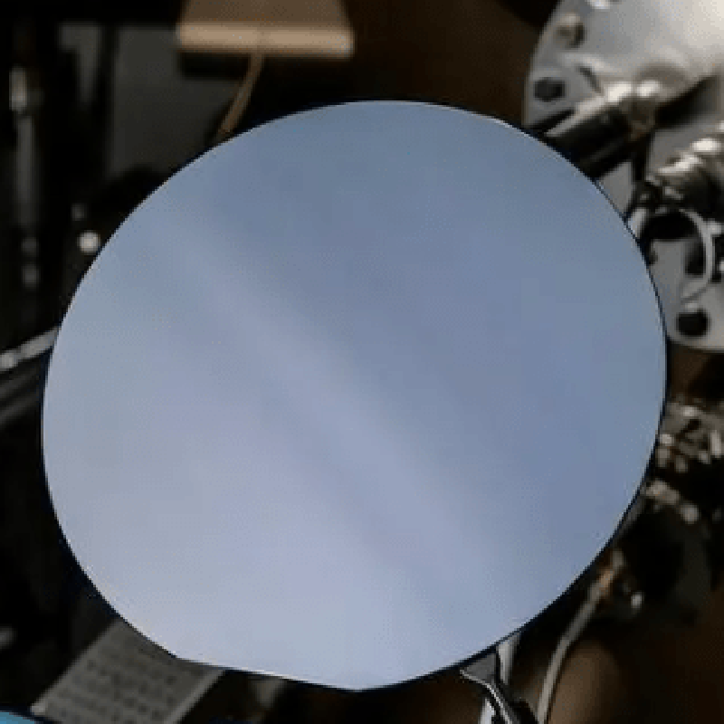
SrTiO3 is a complex oxide compound made up of Strontium, Titanium, and Oxygen. It exhibits semiconducting properties, which is why it’s relevant to the electronics industry. The technology is particularly useful in the development of advanced semiconductor devices such as MOSFETs, solar cells, and transistors, among others.
SrTiO3 wafers have been in use in the semiconductor industry for years, but scientists have been exploring ways to make the compound material more efficient and precise. New research shows that combining SrTiO3 with other materials, such as hafnium oxide, can produce even more remarkable results.
The company behind this breakthrough development is a leading producer of high-quality wafers for the electronics industry. The company has been a pioneer in the development of semiconductor-grade crystals, and its technological advancements continue to push the boundaries of what is possible within the industry.
The SrTiO3 wafer technology has significant implications for the future of the electronics industry. Manufacturers can use the technology to develop devices that are more powerful, efficient, and affordable. The use of SrTiO3 wafers in the manufacturing process ensures that electronic components are more reliable and can operate at higher temperatures.
The technology also has significant benefits for solar cell technology. SrTiO3-based solar cells have higher conversion efficiencies than conventional cells, making them more desirable for use in photovoltaic systems. The use of this technology in solar panels could lead to the development of more efficient and cost-effective solar panels, helping bring clean energy to millions of people worldwide.
The innovative SrTiO3 wafer technology has many applications, including in the automotive, healthcare, and aerospace industries. Researchers are exploring new uses for the technology and hope to discover new applications that will further revolutionize the electronics industry in the coming years.
The company's patented manufacturing process for SrTiO3 wafers ensures the production of high-quality materials that meet strict industry standards. The company's wafers are currently being used in research and development laboratories around the world, and several companies have already adopted the technology in their manufacturing processes.
The use of SrTiO3 wafers in electronic devices is set to increase in the coming years as the technology becomes more widespread and affordable. The introduction of this technology has significant implications for the electronics industry, and researchers are excited by its potential to transform the industry's future.
In conclusion, the emergence of SrTiO3 wafers has set the semiconductor industry on a path towards a new generation of electronic devices. The technology has significant implications for the development of powerful, efficient, and affordable electronic devices, solar cell technology, and many other applications. With continued research and development, the technology has the potential to revolutionize the electronics industry for years to come.
Company News & Blog
Key Developments in the Global Wafers Market: Insights, Trends, and Forecasts
Inp Wafers, a leading semiconductor wafer supplier in Asia, has been making headlines in the tech industry for its innovative products and solutions. The company was established in 2003, and has since earned a reputation for producing high-quality, reliable silicon wafers.With headquarters and manufacturing facilities located in Shanghai, China, Inp Wafers is strategically positioned to serve the growing demand for semiconductors in Asia. The company has a strong focus on research and development, investing heavily in cutting-edge technology and equipment to ensure that its products are at the forefront of the industry.Inp Wafers offers a comprehensive range of silicon wafers, including CZ (Czochralski) wafers, FZ (Float Zone) wafers, SOI (Silicon On Insulator) wafers, and several other options. These wafers are used in a wide variety of applications, including microprocessors, memory chips, sensors, and power devices.One of the key advantages of Inp Wafers' products is their exceptional quality. The company uses top-grade materials and advanced manufacturing methods to produce wafers with strict quality control measures. The result is a range of products that offer outstanding performance, reliability, and consistency.Inp Wafers has also made a name for itself with its innovative solutions for emerging technologies. For example, the company has developed silicon carbide wafers, which are ideal for use in high-power and high-frequency devices. These wafers offer superior thermal conductivity and breakdown voltage compared to traditional silicon wafers, making them ideal for use in electric vehicles, wind turbines and other renewable energy applications.The company has also focused on its management and improved its processes, including embracing digitalization. The company leverages advanced software tools like Enterprise Resource Planning (ERP) and Customer Relationship Management (CRM) systems to streamline its operations and make it easier for customers to place orders and receive technical support.Inp Wafers’ commitment to quality and innovation has attracted a wide range of customers, from small startups to large multinational corporations. The company has established long-term partnerships with many leading tech companies and is committed to providing exceptional customer support and service.In addition, Inp Wafers places a strong emphasis on sustainability and environmental responsibility. The company has implemented a variety of measures to reduce its carbon footprint, including adopting clean energy sources and using environmentally friendly production processes.Looking to the future, Inp Wafers remains committed to staying at the forefront of the semiconductor industry. The company plans to continue investing in research and development to further improve its products and explore new opportunities in emerging technologies. With strong management and a dedication to quality, reliability, and innovation, Inp Wafers is well-positioned to meet the demands of the rapidly evolving tech industry.
Advanced Crystal Ingot Technologies Discovered for Enhanced Laser Applications
**Title: Groundbreaking YAG Crystal Ingot Revolutionizes the Semiconductor Industry***Date: [Insert Date]**Location: [Insert Location]**Introduction*In a groundbreaking development, a revolutionary YAG Crystal Ingot has emerged on the market, transforming the semiconductor industry. This high-performance crystal ingot, developed by [Company Name], promises to elevate the efficiency and functionality of electronic devices to unprecedented levels. With its exceptional properties, the YAG Crystal Ingot is poised to revolutionize various sectors, including telecommunications, consumer electronics, and even medicine.*Company Overview*[Company Name], a leading innovator in the field of advanced materials, has established itself as a pioneer in developing cutting-edge technologies. Focused on pushing the boundaries of what is possible, the company has constantly strived to develop solutions that address the evolving needs of industries globally. Their relentless pursuit of excellence has earned them a prominent position, with their products being used extensively across various sectors.*YAG Crystal Ingot: The Game Changer*The YAG Crystal Ingot, developed by [Company Name]'s team of brilliant scientists and engineers, has created a buzz in the semiconductor manufacturing domain. This crystal ingot is made from yttrium aluminum garnet, or YAG, which exhibits exceptional optical and thermal properties. The unique combination of these properties enables the YAG Crystal Ingot to outperform existing semiconductor materials in several key aspects.One of the most significant advantages of the YAG Crystal Ingot is its outstanding thermal conductivity. High thermal conductivity is essential in semiconductor applications, as it aids in efficiently dissipating heat generated during device operation. The YAG Crystal Ingot, thanks to its superior thermal conductivity, ensures that electronic devices can operate at higher power levels without the risk of overheating, ultimately boosting their performance and longevity.Additionally, the YAG Crystal Ingot's optical properties allow for enhanced light transmission, making it perfect for applications in optoelectronic devices such as lasers, LEDs, and optical amplifiers. Its ability to efficiently transmit light across a broad spectrum enables manufacturers to create more efficient and reliable devices, benefiting industries such as telecommunications, data centers, and medical diagnostics.Moreover, the YAG Crystal Ingot exhibits exceptional mechanical properties, offering superior resistance to shocks and vibrations. This resilience makes it an ideal material for manufacturing devices meant for rugged environments or those subjected to constant movement, such as aerospace and defense equipment.The outstanding performance of the YAG Crystal Ingot is a testament to [Company Name]'s commitment to advancing technology and delivering innovative solutions. Their investment in research and development has allowed them to overcome the limitations of traditional materials and introduce a game-changing semiconductor product.*Envisioning the Future*The implications of the YAG Crystal Ingot's development are profound and far-reaching. Industries that rely heavily on semiconductor technology, such as telecommunications, consumer electronics, automotive, and healthcare, will experience a paradigm shift with the integration of this advanced material.Telecommunications companies will benefit from the YAG Crystal Ingot's ability to enhance the overall efficiency and reliability of their networks. Faster data transfer, lower latency, and improved signal quality will improve the end-user experience and lay the groundwork for the future of connectivity.Consumer electronics will witness a new era of technological advancements, with devices that exhibit higher performance, improved energy efficiency, and longer lifespans. From smartphones to smart home devices, the integration of YAG Crystal Ingot will elevate the functionality and durability of these products, delighting consumers across the globe.The medical field will also embrace the YAG Crystal Ingot, as it offers groundbreaking opportunities for better diagnostic tools, advanced surgical equipment, and the development of innovative health monitoring devices. Improved precision, reliability, and safety will revolutionize patient care and enable medical professionals to achieve groundbreaking breakthroughs.*Conclusion*With the introduction of the YAG Crystal Ingot, [Company Name] has truly changed the game in the semiconductor industry. This remarkable crystal ingot's superior thermal conductivity, optical properties, and mechanical resilience make it an invaluable material for various applications. By leveraging the potential of the YAG Crystal Ingot, industries can elevate their performance, redefine technological norms, and ultimately shape a future that is brighter, faster, and more efficient than ever before.
New breakthrough in manufacturing process of computer processors using silicon wafer technology
Silicon Wafer Chips Revolutionize Semiconductor IndustryThe semiconductor industry, which lies at the heart of technological advancements, is constantly striving to push the boundaries of innovation. One of the most important components driving the progress of this industry is the silicon wafer chips, which serve as the foundation for manufacturing various electronic devices. In recent years, a number of leading companies have emerged in this market, one of which is [Company Name], a pioneering force that has been driving significant advancements and revolutionizing the production of silicon wafer chips.[Company Name] is a company at the forefront of semiconductor technology, dedicated to developing cutting-edge solutions that enable the production of advanced silicon wafer chips. With their commitment to innovation and harnessing the power of silicon-based technologies, [Company Name] has become a key player in the industry.Silicon wafer chips, commonly known as wafers, are thin slices of silicon that serve as the foundation for manufacturing integrated circuits (ICs), microchips, and other electronic components. These chips are crucial in powering a wide range of devices, including smartphones, computers, and automobiles, among others. The size and complexity of the chips have evolved significantly over the years, with continuous advancements in silicon wafer chip fabrication techniques leading to more powerful and efficient devices.[Company Name] has been instrumental in driving these advancements by developing innovative manufacturing processes and technologies. Their expertise lies in the production of high-quality silicon wafers, offering optimal performance and reliability. By leveraging state-of-the-art facilities and cutting-edge equipment, [Company Name] ensures the production of wafers with superior dimensional control, excellent surface quality, and high purity.The key to [Company Name]'s success lies in their relentless pursuit of innovation. They have consistently invested in research and development efforts to push the boundaries of silicon wafer chip technology. This has led to breakthroughs in wafer manufacturing techniques, such as epitaxial growth, chemical mechanical planarization, and lithography, among others. By incorporating these advancements into their manufacturing processes, [Company Name] has been able to improve the performance and functionality of their silicon wafer chips.Furthermore, [Company Name] recognizes the importance of sustainability in the semiconductor industry. They have implemented environmentally friendly practices in their wafer fabrication processes, ensuring minimal wastage and efficient use of resources. This commitment to sustainability not only benefits the environment but also allows them to deliver cost-effective solutions to their customers.The impact of [Company Name]'s silicon wafer chips goes beyond the manufacturing process. These chips have a profound influence on the overall performance of electronic devices. Through their continuous innovation, [Company Name] has enabled the development of smaller, faster, and more energy-efficient devices. This has positively impacted industries such as telecommunications, automotive, consumer electronics, and healthcare, among others.Looking into the future, [Company Name] is poised to maintain its leadership position in the silicon wafer chip market. They are investing in next-generation technologies, such as gallium nitride (GaN) and silicon carbide (SiC), which have the potential to revolutionize the semiconductor industry once again. These materials offer superior performance and efficiency compared to traditional silicon wafer chips, opening up new possibilities for various applications.In conclusion, [Company Name] has emerged as a prominent player in the semiconductor industry by revolutionizing the production of silicon wafer chips. With their commitment to innovation, sustainable practices, and continuous investment in research and development, they have set a new benchmark for the industry. Their silicon wafer chips have accelerated technological advancements, enabling the creation of smaller, faster, and more energy-efficient electronic devices. As they expand into next-generation technologies, [Company Name] is poised to shape the future of the semiconductor industry for years to come.
High-Quality Wafer Fabrication: LiNbO3 and LiTaO3
LiNbO3/LiTaO3 Wafer - The next frontier of semiconductor technologyA new age of semiconductor technology is about to dawn with the introduction of the LiNbO3/LiTaO3 wafer. As the world is progressing towards smaller and faster electronic devices, the limitations of conventional silicon-based semiconductor technology have become increasingly apparent. In this context, LiNbO3/LiTaO3 wafer technology holds great promise by offering many advantages over silicon-based semiconductor technology.The LiNbO3/LiTaO3 wafer technology is based on the use of Lithium Niobate or Lithium Tantalate as the substrate material. These materials have several unique properties, such as high electro-optic coefficient, low acoustic loss, high piezoelectric coefficient, and low dielectric constant, which make them ideal for a wide range of applications, including optoelectronics, acoustoelectronics, and microwave technologies.One of the key advantages of LiNbO3/LiTaO3 wafer technology over silicon-based semiconductor technology is its high-speed performance. The high electro-optic coefficient of LiNbO3/LiTaO3 wafers allows for ultra-fast modulation and switching of light signals. As a result, LiNbO3/LiTaO3 wafer technology is widely used in optoelectronic devices, such as lasers, modulators, and detectors, where high-speed operation is crucial.Another advantage of LiNbO3/LiTaO3 wafer technology is its high-frequency performance. The low acoustic loss and high piezoelectric coefficient of Lithium Niobate and Lithium Tantalate make them ideal for the fabrication of acoustic devices, such as surface acoustic wave (SAW) filters and resonators. These devices are widely used in mobile communication, satellite communication, and radar systems, where high-frequency performance is of utmost importance.Furthermore, LiNbO3/LiTaO3 wafer technology offers superior thermal and mechanical stability compared to silicon-based semiconductor technology. The low dielectric constant of Lithium Niobate and Lithium Tantalate reduces the parasitic capacitance and improves the signal-to-noise ratio of electronic devices. This makes them suitable for harsh environmental conditions, such as high-temperature and high-pressure environments.The potential applications of LiNbO3/LiTaO3 wafers are vast, ranging from optoelectronics and acoustoelectronics to microwave technologies. One of the most promising applications of LiNbO3/LiTaO3 wafer technology is in the field of quantum computing. The high-speed and low-noise properties of LiNbO3/LiTaO3 wafers make them ideal for the fabrication of quantum gates and qubits, which are the building blocks of quantum computers.In light of these advantages, the market for LiNbO3/LiTaO3 wafers is set to grow exponentially in the coming years. The global LiNbO3/LiTaO3 wafer market is projected to reach USD 1.2 billion by 2025, growing at a CAGR of 7.5% from 2020 to 2025. This growth can be attributed to the increasing demand for high-speed and high-frequency electronic devices in various industries, such as telecommunications, aerospace, defense, and healthcare.At the forefront of LiNbO3/LiTaO3 wafer technology is our company. We are a leading manufacturer and supplier of high-quality LiNbO3/LiTaO3 wafers, offering a wide range of sizes and specifications to meet the diverse needs of our customers. Our state-of-the-art facilities, advanced equipment, and experienced team enable us to deliver wafers with exceptional quality and performance.We pride ourselves on providing our customers with customized solutions tailored to their specific needs, whether it is for R&D or mass production. Our commitment to quality, reliability, and customer satisfaction has earned us a reputation as a trusted partner in the semiconductor industry.In conclusion, the LiNbO3/LiTaO3 wafer technology is poised to revolutionize the semiconductor industry by offering high-speed, high-frequency, and high-performance electronic devices. With our expertise and commitment to innovation and excellence, we are well-positioned to meet the growing demand for LiNbO3/LiTaO3 wafers and contribute to the advancement of semiconductor technology.
Sic Chip Market Witnesses Steady Growth Amid Increasing Demand
Sic Chip: Revolutionizing Industries with Enhanced Performance and Efficiency[Company Name], a leader in technological innovation, has recently unveiled its latest breakthrough – the Sic Chip. With cutting-edge features and unparalleled performance, this revolutionary chip has the potential to transform various industries, paving the way for a future of improved efficiency and productivity.The Sic Chip, short for Silicon Carbide Chip, is a significant advancement in semiconductor technology. Unlike conventional silicon chips, Sic Chips are composed of silicon carbide, a compound with superior thermal conductivity and a wider bandgap. This unique composition allows the chip to perform more efficiently at higher temperatures, making it ideal for applications that require robust performance in extreme environments.One of the key advantages of the Sic Chip is its ability to handle higher voltages and currents, making it a game-changer for power electronics. This chip has significantly lower power losses and can operate at higher frequencies than traditional silicon chips. As a result, it is highly sought after by manufacturers in the automotive, aerospace, and energy sectors. The automotive industry, in particular, stands to benefit greatly from the Sic Chip, as it enables the development of more efficient electric vehicles with longer battery life and faster charging capabilities.Furthermore, the Sic Chip's enhanced power efficiency reduces the need for complex cooling systems, leading to cost savings and reduced environmental impact. In power conversion applications, the chip's superior performance allows for smaller and lighter systems. This is particularly advantageous in the renewable energy sector, where space constraints and weight limitations are critical factors.Another area where the Sic Chip is making significant inroads is in the field of telecommunications. The chip's ability to handle high power densities and operate at high temperatures makes it an ideal choice for base station applications. With the increasing demand for 5G networks, the efficiency and reliability offered by the Sic Chip are highly valued by telecommunication companies.The SiC Chip is also revolutionizing the computing industry. Its exceptional thermal conductivity enables faster heat dissipation, leading to improved performance and reliability in high-performance computing applications. From data centers to supercomputers, the Sic Chip is paving the way for more powerful and efficient computing systems.In addition to the technical advantages, [Company Name]'s Sic Chip also holds a competitive edge in terms of production capabilities. The company has developed a highly efficient manufacturing process that ensures high-quality chips with excellent yields. This puts [Company Name] at the forefront of the industry, establishing itself as a reliable and trusted provider of Sic Chips.Commenting on the significance of the Sic Chip, [Company Name]'s CEO stated, "This breakthrough technology has the potential to revolutionize multiple industries, making processes more efficient and sustainable. Our Sic Chip is a clear example of our commitment to driving innovation and delivering cutting-edge solutions that address the challenges of the modern world."As the demand for faster, more efficient and reliable technologies continues to grow, the introduction of the Sic Chip marks a turning point in the semiconductor industry. With its superior performance, enhanced power efficiency, and wider range of applications, this groundbreaking chip is set to shape the future of multiple industries, fueling progress and innovation across the globe. [Company Name] remains at the forefront of this technological revolution, providing innovative solutions that drive the world towards a brighter and more sustainable future.
Understanding the Importance of Substrate in the Semiconductor Industry
In today's fast-paced technological world, the semiconductor industry is constantly advancing with new discoveries and innovations. One of the newest advancements in the field of semiconductors is the substrate technology developed by a leading company in the industry.The unprecedented substrate technology developed by this company has revolutionized the way in which semiconductors are designed and manufactured. The substrate technology, which is used in a variety of electronic devices, enhances the performance of semiconductors by improving their speed, power efficiency, and overall functionality.Substrates are an essential component in the production of semiconductors, as they provide the foundation on which the semiconductor is built. The development of this new substrate technology, therefore, marks a major milestone in the industry, as it offers a significant improvement to the already existing substrate technology.The substrate technology developed by this company uses advanced materials and advanced manufacturing processes to create a highly efficient and high-performance substrate. The technology is based on a new type of substrate material that incorporates a number of cutting-edge design features, making it an ideal component for a range of electronic devices.The company's substrate technology has been specifically designed to meet the demands of modern electronics, such as smartphones, tablets, and power modules. With the increase in the number of electronic devices being used worldwide, there is now a greater demand for components that provide greater functionality and efficiency. This substrate technology is one such technology, offering improved performance, durability, and reliability in electronic devices.Furthermore, the new substrate technology provides a cost-effective solution for the manufacturing of semiconductors, enabling manufacturers to produce semiconductors more efficiently and at a lower cost. This technology, therefore, not only benefits the manufacturers but also benefits the end-users by driving down the cost of electronic devices.The company that has developed this revolutionary substrate technology has been in the semiconductor industry for over a decade. With a team of experienced professionals, they have made significant contributions to the development of a range of innovative semiconductor products.Their commitment to research and development has resulted in numerous breakthroughs in the field of semiconductor technology. Their latest development of the substrate technology is a testament to their expertise and dedication to creating products that meet the needs of the modern world.Looking to the future, this company continues to invest in research and development initiatives that will lead to further advancements in the field of semiconductor technology. As the industry advances, the company remains committed to developing innovative products that will set a new standard for performance, reliability, and functionality.Overall, the new substrate technology developed by this company is a significant advancement in the semiconductor industry. The technology is set to transform the way in which semiconductors are designed and manufactured, offering a cost-effective, high-performance solution that will benefit both manufacturers and end-users alike.With an experienced team of professionals and a commitment to research and development, this company is poised to remain at the forefront of the semiconductor industry for years to come. Their innovation and expertise continue to drive advancements in the field, creating products that will shape the future of technology.
Large Crystal Ingot of Lithium Tantalate (LiTaO3) Developed for Advanced Electronics
LiTaO3 Ingot: A Next-Generation Material for the FutureIn today's fast-paced world, technology has become an integral part of our daily lives. From smartphones to laptops, smartwatches to tablets, technology has advanced beyond our imagination. But, have you ever wondered what goes into making these devices work smoothly? The answer lies in the materials used to create them. One such material is LiTaO3 Ingot.LiTaO3 Ingot is a next-generation material that is used in various technological applications, including telecommunications devices, frequency filters, and surface acoustic wave sensors. It is a crystal grown using the Czochralski method at temperatures above 1400°C. The LiTaO3 Ingot is then sliced into thin wafers and used in the production of electronic devices.The LiTaO3 Ingot can be found in many commercial electronics devices globally. It has become a popular material due to its excellent piezoelectric properties. Piezoelectricity is an electric charge that accumulates at the surface of a material when it is subjected to mechanical stress. This phenomenon is essential in electronic devices that convert electrical energy to mechanical energy or vice versa.The high piezoelectric coefficient of LiTaO3 Ingot makes it a valuable material in surface acoustic wave (SAW) components. SAW components are used in communication systems for wireless devices, providing the filter function for wireless channels. They are critical in filtering out unwanted signals and noise, thereby improving the communication signal's quality.Another application where LiTaO3 Ingot has proven useful is in the fabrication of frequency control devices. Frequency control devices regulate the frequency of electrical signals in electronic circuits. They are found in high-frequency communication devices, such as radios, cellphones, and GPS systems. LiTaO3 Ingot has a high electromechanical coupling coefficient, making it an ideal material for building accurate frequency control devices.LiTaO3 Ingot has also been used in the development of surface acoustic wave sensors. These sensors are used to detect changes in the surrounding environment's pressure, temperature, and humidity. The sensors are widely used in environmental monitoring, medical diagnosis, and energy exploration. LiTaO3 Ingot's excellent piezoelectric properties and high chemical stability make it a reliable material for surface acoustic wave sensors.{Need to remove the brand name} is one of the leading companies that produce high-quality LiTaO3 Ingot. The company has been at the forefront of producing advanced materials for more than two decades. Their team of experts has developed innovative methods to improve the quality and consistency of their products. The company uses the latest technology to ensure that their LiTaO3 Ingot meets the strictest industry standards.{Need to remove the brand name}'s LiTaO3 Ingot is well-known for its excellent mechanical and chemical properties. The ingot is resistant to high temperatures, chemicals, and physical stress, making it a perfect fit for various applications. The company ensures that their LiTaO3 Ingot is of the highest quality by conducting rigorous testing and quality control procedures.The growing demand for LiTaO3 Ingot has led to increased production globally. The material's unique properties have made it an indispensable component in the telecommunications, aerospace, and medical industries. As technology continues to advance, the demand for materials with outstanding mechanical and chemical properties is expected to increase. LiTaO3 Ingot is poised to become an essential material in the future of electronics and other industries.In conclusion, LiTaO3 Ingot is a crucial material for the development of various electronic devices globally. Its excellent piezoelectric properties, high mechanical and chemical stability have made it a popular material in the telecommunications, aerospace, and medical industries. {Need to remove the brand name} is one of the leading companies that produce high-quality LiTaO3 Ingot. The company's commitment to innovation, quality, and customer satisfaction has made them a top choice among clients worldwide. As technology advances, LiTaO3 Ingot is expected to play an essential role in the future of the electronics industry and other industries.
Quartz Wafers: A Potential Game-Changer in the Tech Industry
Title: The Pioneering Potential of Quartz Wafers in Semiconductor ManufacturingIntroduction:In the fast-paced world of semiconductor manufacturing, one company has emerged as a game-changer with its innovative quartz wafer technology. Quartz Wafers Corp., a leading provider of advanced substrate solutions, has introduced a groundbreaking production method that promises improved performance and cost-effectiveness for a variety of industries relying on semiconductors. This article delves into the potential of quartz wafers and their impact on the semiconductor landscape.Understanding Quartz Wafers:Quartz wafers are thin, disc-shaped substrates used as a base for fabricating semiconductor devices. Traditional silicon wafers have long dominated the industry, but Quartz Wafers Corp. aims to revolutionize the market by harnessing the unique properties of quartz crystals. Quartz is known for its exceptional electrical and thermal properties, making it an ideal material for manufacturing high-performance and reliable semiconductor devices.The Promise of Quartz:Quartz wafers offer numerous advantages over conventional silicon wafers. Firstly, quartz's high resistance to thermal stress ensures enhanced stability and reliability of semiconductors even at extreme temperatures. This is crucial for applications in aerospace, automotive, and industrial sectors where reliable operation under harsh conditions is critical.Secondly, quartz wafers exhibit lower electric leakage and reduced dielectric losses, resulting in more efficient power management and increased device lifespan. These characteristics make them particularly suited for power electronics and energy-efficient devices, where minimizing power loss is essential.Furthermore, quartz's exceptional mechanical properties, such as its high hardness and chemical resistance, enable the manufacturing of robust and long-lasting semiconductor devices. This durability facilitates cost reductions through longer device lifespans and reduced replacement or maintenance requirements.Quartz Wafers Corp.'s Innovative Manufacturing Technique:Quartz Wafers Corp.'s manufacturing process sets it apart from its competitors. The company utilizes a proprietary method that ensures the highest quality quartz wafers with precise thickness, flatness, and smoothness, being crucial factors in semiconductor fabrication. By leveraging advanced manufacturing techniques, Quartz Wafers Corp. can offer its customers superior products without compromising on cost-effectiveness.Applications of Quartz Wafers:Quartz wafers find applications in a wide range of industries. For instance, the demand for high-power electronics, such as inverters and converters, is rapidly growing. Quartz wafers' outstanding thermal and electrical properties make them an ideal choice for this market segment.Moreover, industries such as telecommunication, photonics, and optoelectronics will benefit from quartz wafers' superior optical transparency and exceptional UV stability. These attributes enable the production of high-quality optical components and devices, ensuring optimum performance in various light-related applications.Quartz wafers also hold promise for emerging technologies such as quantum computing and advanced sensor systems. Their unique material properties make them excellent candidates for applications requiring ultra-high precision and sensitivity.Conclusion:Quartz Wafers Corp.'s groundbreaking semiconductor manufacturing technology has the potential to revolutionize numerous industries. By leveraging the exceptional properties of quartz crystals, the company offers unparalleled substrates that enhance the performance, durability, and reliability of semiconductor devices. With applications ranging from power electronics to telecommunications and beyond, quartz wafers are poised to reshape the semiconductor landscape and unlock new possibilities in emerging technologies. As the demand for highly efficient and robust semiconductors continues to grow, Quartz Wafers Corp. stands at the forefront, ready to make a lasting impact.
Exploring the Advantages of Silicon on Sapphire Technology in Cutting-Edge Innovations
Silicon-On-Sapphire (SOS), a revolutionary technology used in making semiconductors, has emerged as a promising solution for high-frequency wireless communication and high-speed digital circuits. SOS is an advanced technology used in manufacturing electronic devices that are faster, more reliable, and efficient than traditional silicon-based technologies. This technology is highly sought after by manufacturers worldwide, and one company is leading the way in bringing it to the forefront – Skyworks Solutions.Skyworks Solutions, Inc. (need remove brand name) is a company that is committed to making cutting-edge products that help connect people around the world. One of their main products is radio frequency integrated circuits (RFICs), which are critical components in wireless communication devices, including smartphones, tablets, and IoT devices. For over 20 years, Skyworks has been at the forefront of RFIC production, and now they are leveraging the power of SOS to take their products to the next level.What is Silicon-On-Sapphire?Before we delve into some of the amazing things that Skyworks is doing with SOS technology, let's first take a moment to understand what SOS is. SOS is a type of material used in the production of semiconductors. The material is essentially a layer of silicon deposited on top of a substrate of sapphire. The combination of these two materials creates a stable and durable platform on which to build electronic devices.SOS has several advantages over traditional silicon-based technologies. For one, it has a higher electron mobility, which means that electrons can move more quickly and with less resistance. This increased electron mobility makes SOS ideal for high-frequency wireless communication and high-speed digital circuits, both of which require fast and reliable data transmission.Another advantage of SOS is that it has a higher breakdown voltage than silicon. This means that it can handle higher voltages without becoming damaged. This makes SOS ideal for use in high-power applications.Skyworks Solutions: Using SOS to Create Cutting-Edge ProductsNow that we've covered the basics of SOS, let's take a look at what Skyworks is doing with this technology. Skyworks has long been a leader in producing RFICs that are used in wireless communication devices. However, with the increasing demand for faster and more reliable data transmission, Skyworks saw an opportunity to leverage the power of SOS to create even better products.One area in which Skyworks is using SOS is in the production of 5G wireless communication devices. 5G is the next generation of wireless communication technology, and it promises to be faster and more reliable than current 4G networks. Skyworks is using SOS to produce RFICs that can handle the increased data rates of 5G, ensuring that users can enjoy faster speeds and more reliable connections.SOS is also being used in the production of IoT devices. IoT devices are becoming increasingly popular, and they require RFICs that can handle the unique demands of these devices. SOS is ideal for IoT devices because it can handle high-frequency signals while consuming less power than traditional silicon-based technologies.Skyworks is also using SOS to create products for the automotive industry. Cars are becoming increasingly connected, and they require RFICs that can handle the demands of these systems. SOS is ideal for automotive applications because it can handle high-temperature environments and can operate reliably in harsh conditions.ConclusionIn conclusion, SOS is an advanced technology that is rapidly gaining popularity in the semiconductor industry. Skyworks Solutions is one company that is leading the way in bringing this technology to the forefront. By leveraging the power of SOS, Skyworks is creating cutting-edge products that are faster, more reliable, and efficient than traditional silicon-based technologies. From 5G wireless communication devices to IoT devices to automotive applications, Skyworks is using SOS to create products that are changing the world as we know it.
Introducing the Latest Breakthrough: 8 Inch Wafer Diameter Revolutionizes the Tech Industry
[Company Introduction]{Insert company name} is a leading global semiconductor manufacturer renowned for its cutting-edge technologies and innovative solutions. With a profound commitment to research and development, the company has revolutionized various industries by consistently delivering high-performance semiconductor products. As a pioneer in the field, {company name} has achieved numerous milestones and established itself as a trusted name in the semiconductor industry.[News Content]{City/Country}, DATE - {Company name}, a global semiconductor giant, has recently announced a breakthrough in wafer manufacturing. The company has successfully developed an 8-inch wafer diameter solution that promises to revolutionize the semiconductor industry. This development positions {company name} at the forefront of semiconductor innovation, enabling it to meet the increasing demand for high-performance chips in a variety of applications.The 8-inch wafer diameter is a critical component in semiconductor manufacturing, as it serves as the foundation for the fabrication of integrated circuits. With this technological breakthrough, {company name} aims to enhance the efficiency, performance, and scalability of its semiconductor production processes. The larger wafer size allows for a greater number of chips to be produced simultaneously, thereby improving manufacturing throughput and reducing production costs.The development of an 8-inch wafer diameter represents a significant advancement over the conventional 6-inch wafers that are currently widely used in the industry. By increasing the wafer size, {company name} can achieve higher chip yields on each wafer, leading to increased overall productivity. Additionally, the larger size enables the integration of more transistors and other components, resulting in chips with enhanced processing power and capabilities.Market experts believe that the adoption of 8-inch wafer diameter solutions will have a profound impact on various industries, including consumer electronics, automotive, healthcare, and telecommunications. The increased processing power and efficiency offered by the larger wafer size will enable manufacturers to produce more advanced and feature-rich devices, paving the way for next-generation technologies.{Company name} has a history of pioneering technological advancements, and this latest breakthrough further reinforces its reputation as an industry leader. Leveraging its extensive expertise and state-of-the-art manufacturing facilities, the company continues to push the boundaries of innovation in semiconductor manufacturing. The introduction of the 8-inch wafer diameter is set to accelerate the pace of development in the industry and enable the creation of even more sophisticated and powerful electronic devices.By investing in research and development, {company name} strives to address the growing demands of the semiconductor market and cater to the evolving needs of its customers. Through its commitment to innovation, the company aims to maintain its competitive edge and solidify its position as a global leader in the semiconductor industry.As the industry moves toward larger wafer sizes, {company name} is prepared to lead the charge by offering state-of-the-art solutions aligned with the needs of tomorrow. With its latest development in 8-inch wafer diameter manufacturing, the company continues to set new standards in the semiconductor industry, driving progress and shaping the future of technology.