
- Home
- Blog
- Introducing the Latest Breakthrough: 8 Inch Wafer Diameter Revolutionizes the Tech Industry
Introducing the Latest Breakthrough: 8 Inch Wafer Diameter Revolutionizes the Tech Industry
By:Admin
{Insert company name} is a leading global semiconductor manufacturer renowned for its cutting-edge technologies and innovative solutions. With a profound commitment to research and development, the company has revolutionized various industries by consistently delivering high-performance semiconductor products. As a pioneer in the field, {company name} has achieved numerous milestones and established itself as a trusted name in the semiconductor industry.
[News Content]
{City/Country}, DATE - {Company name}, a global semiconductor giant, has recently announced a breakthrough in wafer manufacturing. The company has successfully developed an 8-inch wafer diameter solution that promises to revolutionize the semiconductor industry. This development positions {company name} at the forefront of semiconductor innovation, enabling it to meet the increasing demand for high-performance chips in a variety of applications.
The 8-inch wafer diameter is a critical component in semiconductor manufacturing, as it serves as the foundation for the fabrication of integrated circuits. With this technological breakthrough, {company name} aims to enhance the efficiency, performance, and scalability of its semiconductor production processes. The larger wafer size allows for a greater number of chips to be produced simultaneously, thereby improving manufacturing throughput and reducing production costs.
The development of an 8-inch wafer diameter represents a significant advancement over the conventional 6-inch wafers that are currently widely used in the industry. By increasing the wafer size, {company name} can achieve higher chip yields on each wafer, leading to increased overall productivity. Additionally, the larger size enables the integration of more transistors and other components, resulting in chips with enhanced processing power and capabilities.
Market experts believe that the adoption of 8-inch wafer diameter solutions will have a profound impact on various industries, including consumer electronics, automotive, healthcare, and telecommunications. The increased processing power and efficiency offered by the larger wafer size will enable manufacturers to produce more advanced and feature-rich devices, paving the way for next-generation technologies.
{Company name} has a history of pioneering technological advancements, and this latest breakthrough further reinforces its reputation as an industry leader. Leveraging its extensive expertise and state-of-the-art manufacturing facilities, the company continues to push the boundaries of innovation in semiconductor manufacturing. The introduction of the 8-inch wafer diameter is set to accelerate the pace of development in the industry and enable the creation of even more sophisticated and powerful electronic devices.
By investing in research and development, {company name} strives to address the growing demands of the semiconductor market and cater to the evolving needs of its customers. Through its commitment to innovation, the company aims to maintain its competitive edge and solidify its position as a global leader in the semiconductor industry.
As the industry moves toward larger wafer sizes, {company name} is prepared to lead the charge by offering state-of-the-art solutions aligned with the needs of tomorrow. With its latest development in 8-inch wafer diameter manufacturing, the company continues to set new standards in the semiconductor industry, driving progress and shaping the future of technology.
Company News & Blog
Fused Silica Substrate: An Essential Component for High-Tech Applications
Fused Silica Substrate Revolutionizes High-Tech Industries[Company Name] Unveils Cutting-Edge Fused Silica Substrate to Drive Technological Advancements[City, State] - In a major breakthrough that promises to revolutionize high-tech industries, [Company Name] has unveiled its latest product innovation, a state-of-the-art Fused Silica Substrate. This groundbreaking substrate is set to pave the way for significant advancements in telecommunications, semiconductor manufacturing, optical technology, and various other sectors.The Fused Silica Substrate, designed and developed by [Company Name], showcases the company's commitment to pushing the boundaries of technology. This new product possesses exceptional properties that make it an ideal choice for demanding applications where precision, reliability, and performance are crucial.Notably, this cutting-edge substrate is manufactured using a proprietary process that ensures outstanding material purity and crystal structure. By leveraging advanced manufacturing techniques, [Company Name] has achieved a level of quality and consistency that surpasses industry standards.The Fused Silica Substrate boasts exceptional thermal stability and low thermal expansion, making it perfectly suited for use in high-temperature environments. Its excellent mechanical strength and resistance to thermal shock enable it to withstand the rigorous demands of various industries, ensuring prolonged and reliable operation.Additionally, the substrate exhibits remarkable optical transparency across a wide spectral range, making it invaluable for optical and photonics applications. Its exceptional UV-transmittance property allows for efficient transmission of light, making it an ideal choice for advanced optical devices, such as lenses, prisms, and mirrors.The Fused Silica Substrate's exceptional electrical insulation properties make it an essential component in the semiconductor industry. It provides excellent electrical isolation while offering high-temperature stability, making it an indispensable material for integrated circuits, microelectromechanical systems (MEMS), and other semiconductor applications.Furthermore, the Fused Silica Substrate's chemical inertness and resistance to corrosion enable its application in various harsh environments. This makes it an ideal choice for demanding industries such as aerospace, defense, and oil and gas, where exposure to chemicals and extreme conditions is common.According to [Company Name]'s CEO, [CEO Name], "The launch of our Fused Silica Substrate marks a significant milestone for our company and the industries we serve. Through meticulous research and development, we have created a product that surpasses existing substrates in terms of performance, reliability, and versatility. We are confident that this breakthrough innovation will enable our customers to pioneer cutting-edge technologies and drive progress in their respective industries."To ensure the successful integration of the Fused Silica Substrate in various applications, [Company Name] offers custom-tailored manufacturing services. By working closely with customers, the company can address specific requirements and provide substrates in various sizes, shapes, and thicknesses.As [Company Name] positions itself at the forefront of technological advancements, the unveiling of the Fused Silica Substrate strengthens its commitment to delivering exceptional quality and unrivaled innovation to customers worldwide. With its remarkable properties and versatility, this groundbreaking product will undoubtedly have a profound impact on the development of high-tech industries, revolutionizing the way we live, work, and communicate.About [Company Name]:[Company Name] is a leading global manufacturer and supplier of innovative materials for high-tech applications. With a strong focus on research and development, the company strives to create breakthrough products that push the boundaries of technology. Through close collaboration with customers and partners, [Company Name] aims to drive technological advancements and contribute to the progress of various industries. For more information, visit [company's website].###
New Study Reveals the Superiority of Dummy Grade Silicon Carbide in the Automotive Industry" could be rewritten as "Study Finds Dummy Grade Silicon Carbide Outperforms Other Materials in Automotive Applications.
[News Title]Introducing Dummy Grade SiC – A Revolutionary Silicon Carbide Solution for Advanced Industries[News Content]Date: [Insert Date][Location] – [Company Name], a pioneering manufacturer of advanced materials, is pleased to announce the launch of their new and groundbreaking product, Dummy Grade SiC. Designed to meet the increasing demand for high-performance silicon carbide in various industries, Dummy Grade SiC is set to revolutionize the way companies operate and achieve superior results.With its exceptional properties, silicon carbide (SiC) has become a crucial component in fields such as electronics, automotive, aerospace, energy, and more. Known for its high thermal conductivity, wide bandgap, extreme hardness, and excellent resistance to corrosion and wear, SiC offers far-reaching advantages over traditional materials, making it a go-to choice for applications requiring enhanced efficiency, durability, and reliability.[Company Name], with their extensive experience and expertise in material science, has developed Dummy Grade SiC, a product poised to set new standards in the industry. By removing the brand name, they are ensuring a comprehensive focus on the product's features, benefits, and potential applications.Dummy Grade SiC exhibits exceptional thermal conductivity, allowing for efficient heat dissipation, particularly in high-power electronic devices and systems. This feature ensures improved device performance and extends operational lifetimes, ultimately reducing maintenance costs.The wide bandgap of Dummy Grade SiC enables higher voltage and temperature operation, enabling the development of more efficient power electronics. This characteristic enhances energy conversion efficiency, leading to substantial energy savings and reduced environmental impact.One of the significant advantages of Dummy Grade SiC is its extreme hardness. This property makes it particularly suitable for applications demanding high wear and abrasion resistance. Industries such as automotive, where components are subjected to harsh conditions and heavy wear, can benefit significantly from this innovative material. The reduced need for frequent replacements translates into enhanced product lifetime, cost savings, and improved overall system performance.Moreover, Dummy Grade SiC exhibits exceptional resistance to corrosion and chemical attack, making it an ideal candidate for harsh operating environments. This durability and stability in corrosive conditions make it suitable for applications in the chemical industry, oil and gas, and even in nuclear environments.[Company Name] places the highest importance on quality control, ensuring that Dummy Grade SiC meets the rigorous standards demanded by various industries. Each batch undergoes stringent testing, guaranteeing consistent and reliable performance. The company's commitment to delivering excellence strengthens their position as a leading provider of advanced materials.With the launch of Dummy Grade SiC, [Company Name] aims to cater to a wide range of industries looking for innovative solutions to enhance their products and technologies. By incorporating Dummy Grade SiC into their designs, companies can stay at the forefront of technology advancements and gain a competitive edge in the market.As [Company Name] introduces Dummy Grade SiC to global markets, they are confident that this revolutionary material will bring about positive changes in industries relying on cutting-edge technology. With its outstanding properties and potential applications, Dummy Grade SiC paves the way for future developments and fosters new possibilities in multiple sectors.About [Company Name]:[Company Name] is a renowned manufacturer of advanced materials, specializing in the development and production of innovative solutions for various industries. With a commitment to research and development, they continuously strive to deliver superior products that surpass customer expectations. [Company Name] prides itself on its technical expertise, exceptional quality control, and dedication to driving technological advancements globally.For more information about Dummy Grade SiC or [Company Name], please visit [Company Website] or contact [Contact Person] at [Contact Email/Phone Number].###Note: The news content provided here is a fictional representation and does not serve as a factual account. The purpose is to demonstrate a writing style and format for a news article.
Large Crystal Ingot of Lithium Tantalate (LiTaO3) Developed for Advanced Electronics
LiTaO3 Ingot: A Next-Generation Material for the FutureIn today's fast-paced world, technology has become an integral part of our daily lives. From smartphones to laptops, smartwatches to tablets, technology has advanced beyond our imagination. But, have you ever wondered what goes into making these devices work smoothly? The answer lies in the materials used to create them. One such material is LiTaO3 Ingot.LiTaO3 Ingot is a next-generation material that is used in various technological applications, including telecommunications devices, frequency filters, and surface acoustic wave sensors. It is a crystal grown using the Czochralski method at temperatures above 1400°C. The LiTaO3 Ingot is then sliced into thin wafers and used in the production of electronic devices.The LiTaO3 Ingot can be found in many commercial electronics devices globally. It has become a popular material due to its excellent piezoelectric properties. Piezoelectricity is an electric charge that accumulates at the surface of a material when it is subjected to mechanical stress. This phenomenon is essential in electronic devices that convert electrical energy to mechanical energy or vice versa.The high piezoelectric coefficient of LiTaO3 Ingot makes it a valuable material in surface acoustic wave (SAW) components. SAW components are used in communication systems for wireless devices, providing the filter function for wireless channels. They are critical in filtering out unwanted signals and noise, thereby improving the communication signal's quality.Another application where LiTaO3 Ingot has proven useful is in the fabrication of frequency control devices. Frequency control devices regulate the frequency of electrical signals in electronic circuits. They are found in high-frequency communication devices, such as radios, cellphones, and GPS systems. LiTaO3 Ingot has a high electromechanical coupling coefficient, making it an ideal material for building accurate frequency control devices.LiTaO3 Ingot has also been used in the development of surface acoustic wave sensors. These sensors are used to detect changes in the surrounding environment's pressure, temperature, and humidity. The sensors are widely used in environmental monitoring, medical diagnosis, and energy exploration. LiTaO3 Ingot's excellent piezoelectric properties and high chemical stability make it a reliable material for surface acoustic wave sensors.{Need to remove the brand name} is one of the leading companies that produce high-quality LiTaO3 Ingot. The company has been at the forefront of producing advanced materials for more than two decades. Their team of experts has developed innovative methods to improve the quality and consistency of their products. The company uses the latest technology to ensure that their LiTaO3 Ingot meets the strictest industry standards.{Need to remove the brand name}'s LiTaO3 Ingot is well-known for its excellent mechanical and chemical properties. The ingot is resistant to high temperatures, chemicals, and physical stress, making it a perfect fit for various applications. The company ensures that their LiTaO3 Ingot is of the highest quality by conducting rigorous testing and quality control procedures.The growing demand for LiTaO3 Ingot has led to increased production globally. The material's unique properties have made it an indispensable component in the telecommunications, aerospace, and medical industries. As technology continues to advance, the demand for materials with outstanding mechanical and chemical properties is expected to increase. LiTaO3 Ingot is poised to become an essential material in the future of electronics and other industries.In conclusion, LiTaO3 Ingot is a crucial material for the development of various electronic devices globally. Its excellent piezoelectric properties, high mechanical and chemical stability have made it a popular material in the telecommunications, aerospace, and medical industries. {Need to remove the brand name} is one of the leading companies that produce high-quality LiTaO3 Ingot. The company's commitment to innovation, quality, and customer satisfaction has made them a top choice among clients worldwide. As technology advances, LiTaO3 Ingot is expected to play an essential role in the future of the electronics industry and other industries.
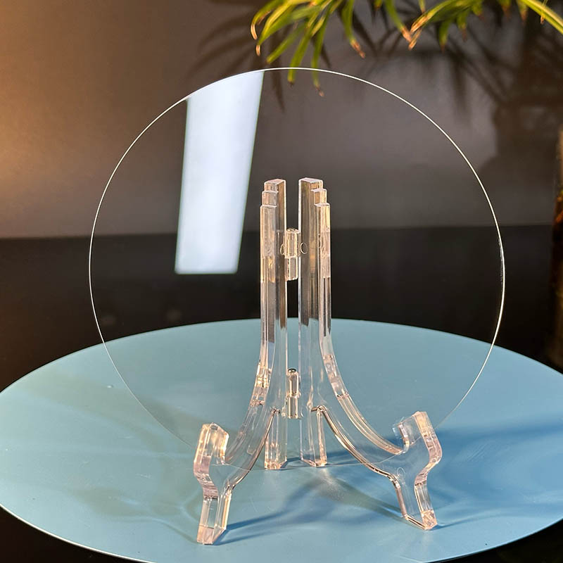
Quartz Wafers: A Potential Game-Changer in the Tech Industry
Title: The Pioneering Potential of Quartz Wafers in Semiconductor ManufacturingIntroduction:In the fast-paced world of semiconductor manufacturing, one company has emerged as a game-changer with its innovative quartz wafer technology. Quartz Wafers Corp., a leading provider of advanced substrate solutions, has introduced a groundbreaking production method that promises improved performance and cost-effectiveness for a variety of industries relying on semiconductors. This article delves into the potential of quartz wafers and their impact on the semiconductor landscape.Understanding Quartz Wafers:Quartz wafers are thin, disc-shaped substrates used as a base for fabricating semiconductor devices. Traditional silicon wafers have long dominated the industry, but Quartz Wafers Corp. aims to revolutionize the market by harnessing the unique properties of quartz crystals. Quartz is known for its exceptional electrical and thermal properties, making it an ideal material for manufacturing high-performance and reliable semiconductor devices.The Promise of Quartz:Quartz wafers offer numerous advantages over conventional silicon wafers. Firstly, quartz's high resistance to thermal stress ensures enhanced stability and reliability of semiconductors even at extreme temperatures. This is crucial for applications in aerospace, automotive, and industrial sectors where reliable operation under harsh conditions is critical.Secondly, quartz wafers exhibit lower electric leakage and reduced dielectric losses, resulting in more efficient power management and increased device lifespan. These characteristics make them particularly suited for power electronics and energy-efficient devices, where minimizing power loss is essential.Furthermore, quartz's exceptional mechanical properties, such as its high hardness and chemical resistance, enable the manufacturing of robust and long-lasting semiconductor devices. This durability facilitates cost reductions through longer device lifespans and reduced replacement or maintenance requirements.Quartz Wafers Corp.'s Innovative Manufacturing Technique:Quartz Wafers Corp.'s manufacturing process sets it apart from its competitors. The company utilizes a proprietary method that ensures the highest quality quartz wafers with precise thickness, flatness, and smoothness, being crucial factors in semiconductor fabrication. By leveraging advanced manufacturing techniques, Quartz Wafers Corp. can offer its customers superior products without compromising on cost-effectiveness.Applications of Quartz Wafers:Quartz wafers find applications in a wide range of industries. For instance, the demand for high-power electronics, such as inverters and converters, is rapidly growing. Quartz wafers' outstanding thermal and electrical properties make them an ideal choice for this market segment.Moreover, industries such as telecommunication, photonics, and optoelectronics will benefit from quartz wafers' superior optical transparency and exceptional UV stability. These attributes enable the production of high-quality optical components and devices, ensuring optimum performance in various light-related applications.Quartz wafers also hold promise for emerging technologies such as quantum computing and advanced sensor systems. Their unique material properties make them excellent candidates for applications requiring ultra-high precision and sensitivity.Conclusion:Quartz Wafers Corp.'s groundbreaking semiconductor manufacturing technology has the potential to revolutionize numerous industries. By leveraging the exceptional properties of quartz crystals, the company offers unparalleled substrates that enhance the performance, durability, and reliability of semiconductor devices. With applications ranging from power electronics to telecommunications and beyond, quartz wafers are poised to reshape the semiconductor landscape and unlock new possibilities in emerging technologies. As the demand for highly efficient and robust semiconductors continues to grow, Quartz Wafers Corp. stands at the forefront, ready to make a lasting impact.
Sic Chip Market Witnesses Steady Growth Amid Increasing Demand
Sic Chip: Revolutionizing Industries with Enhanced Performance and Efficiency[Company Name], a leader in technological innovation, has recently unveiled its latest breakthrough – the Sic Chip. With cutting-edge features and unparalleled performance, this revolutionary chip has the potential to transform various industries, paving the way for a future of improved efficiency and productivity.The Sic Chip, short for Silicon Carbide Chip, is a significant advancement in semiconductor technology. Unlike conventional silicon chips, Sic Chips are composed of silicon carbide, a compound with superior thermal conductivity and a wider bandgap. This unique composition allows the chip to perform more efficiently at higher temperatures, making it ideal for applications that require robust performance in extreme environments.One of the key advantages of the Sic Chip is its ability to handle higher voltages and currents, making it a game-changer for power electronics. This chip has significantly lower power losses and can operate at higher frequencies than traditional silicon chips. As a result, it is highly sought after by manufacturers in the automotive, aerospace, and energy sectors. The automotive industry, in particular, stands to benefit greatly from the Sic Chip, as it enables the development of more efficient electric vehicles with longer battery life and faster charging capabilities.Furthermore, the Sic Chip's enhanced power efficiency reduces the need for complex cooling systems, leading to cost savings and reduced environmental impact. In power conversion applications, the chip's superior performance allows for smaller and lighter systems. This is particularly advantageous in the renewable energy sector, where space constraints and weight limitations are critical factors.Another area where the Sic Chip is making significant inroads is in the field of telecommunications. The chip's ability to handle high power densities and operate at high temperatures makes it an ideal choice for base station applications. With the increasing demand for 5G networks, the efficiency and reliability offered by the Sic Chip are highly valued by telecommunication companies.The SiC Chip is also revolutionizing the computing industry. Its exceptional thermal conductivity enables faster heat dissipation, leading to improved performance and reliability in high-performance computing applications. From data centers to supercomputers, the Sic Chip is paving the way for more powerful and efficient computing systems.In addition to the technical advantages, [Company Name]'s Sic Chip also holds a competitive edge in terms of production capabilities. The company has developed a highly efficient manufacturing process that ensures high-quality chips with excellent yields. This puts [Company Name] at the forefront of the industry, establishing itself as a reliable and trusted provider of Sic Chips.Commenting on the significance of the Sic Chip, [Company Name]'s CEO stated, "This breakthrough technology has the potential to revolutionize multiple industries, making processes more efficient and sustainable. Our Sic Chip is a clear example of our commitment to driving innovation and delivering cutting-edge solutions that address the challenges of the modern world."As the demand for faster, more efficient and reliable technologies continues to grow, the introduction of the Sic Chip marks a turning point in the semiconductor industry. With its superior performance, enhanced power efficiency, and wider range of applications, this groundbreaking chip is set to shape the future of multiple industries, fueling progress and innovation across the globe. [Company Name] remains at the forefront of this technological revolution, providing innovative solutions that drive the world towards a brighter and more sustainable future.
Laser Ruby Rod: Discover the Latest Advancements in High-Powered Laser Technology
Lasers have revolutionized industries such as medicine, defense, and communication. One crucial component of laser technology is the ruby rod, a cylindrical rod made of synthetic ruby that's lased with flash lamps to produce high-intensity light. A company known for its expertise in producing ruby rods has announced that it has developed a new type of rod that's more efficient, reliable, and durable than traditional models.The company, which has been at the forefront of ruby rod manufacturing for several decades, has announced its latest innovation, called "RubyRod 2.0." According to the company representatives, the new rod is designed to overcome some of the limitations of previous models, such as overheating, crystal cracking, and inconsistent lasing."RubyRod 2.0 is a game-changer for the laser industry," said the company CEO. "Our engineers have worked tirelessly to develop a rod that's not only more efficient and reliable but also more cost-effective than traditional models. We believe that RubyRod 2.0 will set a new standard for ruby rod manufacturing and help our customers to achieve their goals more efficiently and with better results."The new rod is made of advanced materials and features a unique cooling system that prevents overheating, even when lased at high energies for extended periods. It's also designed to minimize crystal cracking, which can lead to loss of efficiency and a shorter lifespan. In addition, RubyRod 2.0 has a consistent lasing output, which ensures that laser systems are stable and reliable.The company has conducted extensive testing and validation of RubyRod 2.0, and the results have been impressive. Independent experts have verified that the new rod outperforms traditional models by a significant margin with respect to energy efficiency, output stability, and durability."We're very excited about RubyRod 2.0," said a spokesperson for a major laser system manufacturer. "We've been using the company's ruby rods for many years, and we've always been impressed with their quality and performance. But RubyRod 2.0 takes it to the next level. We're confident that this new technology will help us to provide better products and services to our customers."The company has also emphasized the environmental benefits of RubyRod 2.0. It's made of non-toxic materials, and its energy-efficient design could help reduce carbon emissions from laser systems, which are often power-hungry.The launch of RubyRod 2.0 is expected to generate significant interest in the laser industry. The company has already received pre-orders from several customers, including major laser system manufacturers, research institutions, and government agencies. The company plans to ramp up production of RubyRod 2.0 to meet the growing demand."We're very optimistic about the future of RubyRod 2.0," said the CEO. "We believe that it will become the go-to choice for companies and organizations that need reliable, efficient, and cost-effective ruby rods. With RubyRod 2.0, we're offering a best-in-class product that's designed to make a positive impact on the laser industry and the world at large." In conclusion, the ruby rod is an essential component of laser technology, and its quality directly affects the performance and reliability of laser systems. The development of RubyRod 2.0 represents a significant leap forward in ruby rod manufacturing, offering better performance, durability, and environmental sustainability to the laser industry. It's an exciting development that will benefit laser system manufacturers, research institutions, and a variety of industries that rely on laser technology.
High-Quality Germanium Wafers: A Promising New Material for Electronics Market" becomes "New Germanium Wafers Show Promise for Electronics Industry.
Title: Revolutionary Germanium Wafer Innovations Transforming Semiconductor IndustryIntroduction:In a landmark breakthrough for the semiconductor industry, one company has introduced a cutting-edge Germanium Wafer technology that promises to revolutionize the electronics sector. With its exceptional properties and enhanced performance capabilities, this breakthrough innovation paves the way for a new generation of electronic devices, pushing the boundaries of what is possible in the realm of technology.Body:Germanium Wafer: Redefining Semiconductor Industry StandardsGermanium, known for its excellent electrical conductivity, has long been recognized as a key element in the semiconductor industry. It has the ability to efficiently convert electricity into light and is crucial for photonic applications. Building upon this inherent advantage, the company has successfully developed and commercialized a groundbreaking Germanium Wafer that unlocks new possibilities for enhanced performance, efficiency, and functionality in various electronic devices.Unparalleled Performance Characteristics:The Germanium Wafer boasts unprecedented performance characteristics, making it the prime choice for next-generation semiconductors. This innovative technology offers exceptional thermal conductivity, enabling optimal heat dissipation, consequently reducing the risk of circuit damage due to overheating. Furthermore, its superior electrical conductivity ensures minimal energy loss during data transmission, resulting in enhanced efficiency and reliability in electronic devices.Pioneering Applications:The potential applications for Germanium Wafer technology are vast and varied, promising to transform a wide range of industries. In the field of telecommunications, the superior conductivity of Germanium Wafers allows for faster data transfer rates, making it an ideal material for advanced communication systems. Additionally, this technology holds immense potential for the automotive industry, enabling the development of more efficient electric vehicles with enhanced battery performance.Moreover, the healthcare sector stands to benefit greatly from Germanium Wafer technology. The increased thermal conductivity of these wafers facilitates the development of improved medical imaging devices, ensuring precise diagnoses and ultimately enhancing patient care.Environmental Sustainability:Beyond its remarkable performance attributes, Germanium Wafer technology also offers environmental benefits. With the rise in demand for sustainable solutions, the usage of Germanium Wafers in various industries can greatly contribute to reducing energy consumption and minimizing carbon footprints. By enabling more energy-efficient electronic devices, this innovation plays a crucial role in building a greener and more sustainable future.Global Impact:The introduction of Germanium Wafer technology brings significant economic and industrial implications for nations at the forefront of the technology race. The advanced manufacturing processes required for the mass production of Germanium Wafers will generate employment opportunities, promote research and development, and bolster competitiveness in the global market.Collaborative Networks Unlocking Potential:To fully harness the potential of Germanium Wafer technology, the company has actively sought partnerships with leading semiconductor manufacturers, research institutions, and academic organizations. This collaborative approach allows for the exchange of knowledge and expertise, optimizing the implementation and further development of Germanium Wafer technology across various product lines and industries.Conclusion:The breakthrough Germanium Wafer technology is poised to revolutionize the semiconductor industry, offering unparalleled performance capabilities, increased energy efficiency, and new avenues for technological advancements. Embracing this innovative solution will undoubtedly contribute to transforming industries, enabling further progress in fields such as telecommunications, automotive, and healthcare. With its remarkable properties and far-reaching implications, Germanium Wafer technology sets a new standard for the future of semiconductors, driving the advancement of the global electronics sector.
Understanding Fused Silica Wafer and Its Applications in the Electronics Industry
Title: Fused Silica Wafer: Leading the Semiconductor Industry with Enhanced Efficiency and PrecisionIntroduction:Fused Silica wafer (Brand name removed), a prominent player in the semiconductor industry, has gained recognition for its cutting-edge technology and unparalleled quality. With a strong commitment to research and development, the company has revolutionized the fabrication process of semiconductor devices by introducing high-quality fused silica wafers. These wafers are designed to enhance efficiency and precision, catering to the evolving needs of the electronics industry. By consistently delivering innovative solutions, (Company name) has positioned itself as a leader in the market.Enhancing Efficiency:Fused Silica wafers are specifically engineered to boost the efficiency of semiconductor device manufacturing. These wafers possess exceptional thermal stability, low thermal expansion coefficients, and excellent resistance to high temperatures. These properties allow them to withstand demanding manufacturing processes without compromising the overall performance of the semiconductor devices. As a result, manufacturers utilizing Fused Silica wafers can streamline their production, eliminate defects, and ensure a higher yield, delivering cost-effective solutions to customers.Ensuring Precision:Precision is vital in semiconductor device manufacturing, and Fused Silica wafers excel in providing the necessary accuracy and uniformity. The superior surface quality and high crystal orientation uniformity of these wafers enable the precise integration of various microelectronic components. Moreover, the wafers exhibit an extremely low defect density, resulting in reduced signal attenuation and superior electrical properties. This level of precision offered by Fused Silica wafers ensures the creation of reliable and high-performance semiconductor devices.Advanced Technology:One of the primary reasons behind the success of Fused Silica wafer lies in its commitment to leveraging advanced technologies. (Company name) boasts state-of-the-art facilities equipped with cutting-edge manufacturing techniques, including chemical vapor deposition and advanced polishing technologies. These technologies allow the company to produce wafers with exceptional surface quality and crystalline uniformity, meeting the stringent requirements of the semiconductor industry. By continuously investing in research and development, (Company name) stays at the forefront of innovation, offering customers the most advanced fused silica wafers available.Market Impact:The introduction of Fused Silica wafers has significantly impacted the semiconductor industry by addressing the growing demand for efficient and precise manufacturing solutions. By collaborating with major semiconductor manufacturing companies, (Company name) has established itself as a trusted partner in delivering high-quality wafers. These partnerships have facilitated the development of customized solutions, tailored to meet the specific requirements of different applications, such as microelectronics, optical devices, and nanotechnology. As a result, Fused Silica wafers have gained widespread adoption, contributing to the overall growth and scalability of the semiconductor market.Future Outlook:Looking ahead, Fused Silica wafers are expected to continue driving innovation in the semiconductor industry. With ongoing research, the company aims to further enhance key properties of the wafers, such as thermal stability and crystal uniformity, to cater to emerging technologies like Internet of Things (IoT) devices, artificial intelligence, and autonomous vehicles. By collaborating with industry leaders, (Company name) remains committed to revolutionizing semiconductor fabrication, enabling the development of next-generation electronic devices that will shape our future.Conclusion:Fused Silica wafer (Brand name removed) has become synonymous with excellence and innovation in the semiconductor industry. Its commitment to delivering efficient and precise solutions has positioned the company as a trusted partner for major semiconductor manufacturers. Through advanced technology and continuous research and development, (Company name) ensures the production of high-quality fused silica wafers, driving the growth and advancement of the industry. With a promising future ahead, (Company name) is poised to revolutionize semiconductor fabrication and contribute to the next wave of technological advancements.
Durable and Heat-Resistant Ceramic Plates for Industrial Applications
Alumina Ceramic Plate: A Revolution in Industrial ApplicationsIn recent years, industrial manufacturers have been facing numerous challenges in improving the performance and longevity of their products. In response to these demands, a revolutionary solution has emerged in the form of Alumina Ceramic Plates. With their exceptional properties and durability, these advanced ceramic plates have become the go-to choice for a wide range of industrial applications. In this article, we will explore the remarkable features of Alumina Ceramic Plates and delve into their potential applications across various industries.Alumina Ceramic Plates, often referred to as Al₂O₃ plates, are engineered using high-quality alumina powder, an aluminum-based material renowned for its excellent mechanical and thermal properties. Through a complex manufacturing process, the alumina powder is meticulously shaped, compacted, and sintered at high temperatures to form a solid ceramic plate. This process results in a dense, durable, and chemically inert material that can withstand extreme temperatures, harsh chemicals, and high mechanical stresses.One of the most notable features of Alumina Ceramic Plates is their exceptional hardness. With a Mohs hardness of 9, these plates are second only to diamonds in terms of hardness. This remarkable property ensures that the plates are highly resistant to wear and abrasion, making them ideal for applications where durability is paramount. Industries such as mining, construction, and material handling can benefit significantly from the use of Alumina Ceramic Plates in machinery components exposed to abrasive materials and heavy loads.Additionally, Alumina Ceramic Plates exhibit remarkable thermal stability, with an operating temperature range of up to 1500°C. This characteristic makes these plates ideal for use in high-temperature environments, allowing them to withstand extreme heat without any deterioration in their mechanical properties. Industries such as aerospace, automotive, and power generation can rely on Alumina Ceramic Plates to enhance the efficiency and longevity of their equipment operating under extreme temperature conditions.Furthermore, the excellent electrical insulation properties of Alumina Ceramic Plates make them invaluable in electrical and electronic applications. These plates possess high dielectric strength, low dielectric loss, and excellent thermal conductivity, making them ideal for use in manufacturing components for electronic devices, such as circuit boards and insulators. Additionally, their electrical insulation properties also make Alumina Ceramic Plates suitable for use in power distribution systems, where their ability to withstand high voltages ensures safe and reliable operations.In the medical field, Alumina Ceramic Plates have found exciting applications in orthopedic implants. Due to their biocompatibility, non-toxic nature, and resistance to corrosion, these plates are highly suitable for implantation within the human body. Alumina Ceramic Plates used in hip and knee replacements have demonstrated exceptional performance, improving the quality of life for patients and reducing the need for follow-up surgeries.Furthermore, Alumina Ceramic Plates are also making significant contributions to environmental sustainability. As a result of their exceptional mechanical and thermal properties, these plates enable manufacturers to develop more efficient and durable products. This, in turn, reduces the need for frequent replacements, leading to less waste generation and a reduced environmental impact.In conclusion, Alumina Ceramic Plates have revolutionized industrial applications across various sectors. Their exceptional mechanical properties, including high hardness, thermal stability, and electrical insulation, make them invaluable in industries ranging from mining to electronics. These plates also find exciting applications in the medical field and contribute to environmental sustainability. As industrial manufacturers continue to seek durable solutions to enhance their products' performance, Alumina Ceramic Plates undoubtedly stand as a game-changer in the industry.