
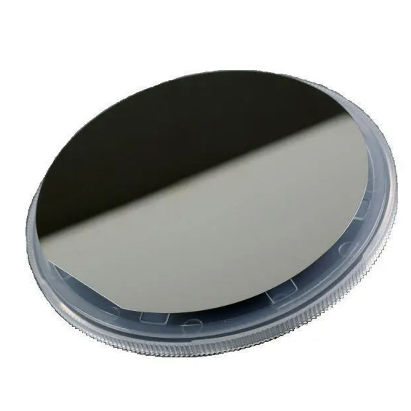
Quartz Wafers: A Potential Game-Changer in the Tech Industry
By:Admin
Introduction:
In the fast-paced world of semiconductor manufacturing, one company has emerged as a game-changer with its innovative quartz wafer technology. Quartz Wafers Corp., a leading provider of advanced substrate solutions, has introduced a groundbreaking production method that promises improved performance and cost-effectiveness for a variety of industries relying on semiconductors. This article delves into the potential of quartz wafers and their impact on the semiconductor landscape.
Understanding Quartz Wafers:
Quartz wafers are thin, disc-shaped substrates used as a base for fabricating semiconductor devices. Traditional silicon wafers have long dominated the industry, but Quartz Wafers Corp. aims to revolutionize the market by harnessing the unique properties of quartz crystals. Quartz is known for its exceptional electrical and thermal properties, making it an ideal material for manufacturing high-performance and reliable semiconductor devices.
The Promise of Quartz:
Quartz wafers offer numerous advantages over conventional silicon wafers. Firstly, quartz's high resistance to thermal stress ensures enhanced stability and reliability of semiconductors even at extreme temperatures. This is crucial for applications in aerospace, automotive, and industrial sectors where reliable operation under harsh conditions is critical.
Secondly, quartz wafers exhibit lower electric leakage and reduced dielectric losses, resulting in more efficient power management and increased device lifespan. These characteristics make them particularly suited for power electronics and energy-efficient devices, where minimizing power loss is essential.
Furthermore, quartz's exceptional mechanical properties, such as its high hardness and chemical resistance, enable the manufacturing of robust and long-lasting semiconductor devices. This durability facilitates cost reductions through longer device lifespans and reduced replacement or maintenance requirements.
Quartz Wafers Corp.'s Innovative Manufacturing Technique:
Quartz Wafers Corp.'s manufacturing process sets it apart from its competitors. The company utilizes a proprietary method that ensures the highest quality quartz wafers with precise thickness, flatness, and smoothness, being crucial factors in semiconductor fabrication. By leveraging advanced manufacturing techniques, Quartz Wafers Corp. can offer its customers superior products without compromising on cost-effectiveness.
Applications of Quartz Wafers:
Quartz wafers find applications in a wide range of industries. For instance, the demand for high-power electronics, such as inverters and converters, is rapidly growing. Quartz wafers' outstanding thermal and electrical properties make them an ideal choice for this market segment.
Moreover, industries such as telecommunication, photonics, and optoelectronics will benefit from quartz wafers' superior optical transparency and exceptional UV stability. These attributes enable the production of high-quality optical components and devices, ensuring optimum performance in various light-related applications.
Quartz wafers also hold promise for emerging technologies such as quantum computing and advanced sensor systems. Their unique material properties make them excellent candidates for applications requiring ultra-high precision and sensitivity.
Conclusion:
Quartz Wafers Corp.'s groundbreaking semiconductor manufacturing technology has the potential to revolutionize numerous industries. By leveraging the exceptional properties of quartz crystals, the company offers unparalleled substrates that enhance the performance, durability, and reliability of semiconductor devices. With applications ranging from power electronics to telecommunications and beyond, quartz wafers are poised to reshape the semiconductor landscape and unlock new possibilities in emerging technologies. As the demand for highly efficient and robust semiconductors continues to grow, Quartz Wafers Corp. stands at the forefront, ready to make a lasting impact.
Company News & Blog
Revolutionary Breakthrough: Researchers Discover the Power of a Single Metal Crystal
Single Metal Crystal Develops Groundbreaking Technology for the Industry [City], [Date] - Single Metal Crystal (SMC), a leading innovator in the technology field, has announced a groundbreaking advancement that is expected to revolutionize the industry. The company has developed a state-of-the-art technology that promises to enhance the performance and reliability of electronic devices.Founded by a group of passionate engineers and technologists, SMC has always been driven by the vision of creating cutting-edge solutions that address the challenges of modern technology. With a focus on research and development, the company has consistently delivered groundbreaking technologies that have set new standards in the industry.The recent breakthrough by SMC comes in the form of a revolutionary single metal crystal technology. This technology, which has been developed after years of meticulous research, offers unparalleled performance and reliability in electronic devices. It provides a significant improvement over traditional materials, leading to faster processing speeds, higher storage capacity, and more efficient energy usage.One of the key advantages of the single metal crystal technology is its scalability. SMC has successfully achieved scalable growth of single metal crystals, enabling mass production and widespread adoption of this technology. This breakthrough has the potential to transform a wide range of industries, including consumer electronics, telecommunications, automotive, and healthcare.The applications of this technology are virtually limitless. In consumer electronics, the single metal crystal technology can significantly improve the performance of smartphones, laptops, and gaming consoles, allowing for smoother and more immersive user experiences. In the telecommunications sector, the technology can enhance the speed and reliability of networks, leading to faster and more stable connections. Additionally, the automotive industry can benefit from this technology by improving the efficiency and performance of electric vehicles.Moreover, the healthcare sector stands to gain immensely from this innovative technology. Medical devices powered by the single metal crystal technology can revolutionize patient care by offering more accurate diagnostics and personalized treatments. Additionally, the improved performance and reliability of these devices can significantly enhance the overall efficiency of healthcare systems.Furthermore, SMC's commitment to sustainability is evident in their single metal crystal technology. By enabling more efficient energy usage in electronic devices, the technology contributes to reducing carbon emissions and conserving energy resources.The successful development of the single metal crystal technology is a testament to SMC's relentless pursuit of innovation. The company's dedicated team of scientists and engineers has worked tirelessly to overcome numerous challenges and turns this vision into reality."Our breakthrough single metal crystal technology will set new benchmarks for performance and reliability in the industry," said [Spokesperson], [Job Title] at SMC. "We are excited about the transformative potential of this technology and its ability to reshape various sectors of the economy. Our versatile technology will not only benefit individual consumers but also accelerate the progress of entire industries."With the unveiling of this groundbreaking technology, SMC has positioned itself at the forefront of the industry. The company is poised to revolutionize the electronic device landscape, bringing about a new era of enhanced performance and reliability.Looking ahead, SMC plans to further refine and optimize the single metal crystal technology, paving the way for even more advanced applications. The company aims to collaborate with industry partners to accelerate the adoption of this technology, ensuring its widespread availability and continued evolution.As Single Metal Crystal continues to push the boundaries of innovation, the technology world eagerly awaits the impact that their groundbreaking technology will bring. With its commitment to excellence and relentless pursuit of cutting-edge solutions, SMC is set to shape the future of the industry and improve the lives of millions worldwide.
Advanced Crystal Ingot Technologies Discovered for Enhanced Laser Applications
**Title: Groundbreaking YAG Crystal Ingot Revolutionizes the Semiconductor Industry***Date: [Insert Date]**Location: [Insert Location]**Introduction*In a groundbreaking development, a revolutionary YAG Crystal Ingot has emerged on the market, transforming the semiconductor industry. This high-performance crystal ingot, developed by [Company Name], promises to elevate the efficiency and functionality of electronic devices to unprecedented levels. With its exceptional properties, the YAG Crystal Ingot is poised to revolutionize various sectors, including telecommunications, consumer electronics, and even medicine.*Company Overview*[Company Name], a leading innovator in the field of advanced materials, has established itself as a pioneer in developing cutting-edge technologies. Focused on pushing the boundaries of what is possible, the company has constantly strived to develop solutions that address the evolving needs of industries globally. Their relentless pursuit of excellence has earned them a prominent position, with their products being used extensively across various sectors.*YAG Crystal Ingot: The Game Changer*The YAG Crystal Ingot, developed by [Company Name]'s team of brilliant scientists and engineers, has created a buzz in the semiconductor manufacturing domain. This crystal ingot is made from yttrium aluminum garnet, or YAG, which exhibits exceptional optical and thermal properties. The unique combination of these properties enables the YAG Crystal Ingot to outperform existing semiconductor materials in several key aspects.One of the most significant advantages of the YAG Crystal Ingot is its outstanding thermal conductivity. High thermal conductivity is essential in semiconductor applications, as it aids in efficiently dissipating heat generated during device operation. The YAG Crystal Ingot, thanks to its superior thermal conductivity, ensures that electronic devices can operate at higher power levels without the risk of overheating, ultimately boosting their performance and longevity.Additionally, the YAG Crystal Ingot's optical properties allow for enhanced light transmission, making it perfect for applications in optoelectronic devices such as lasers, LEDs, and optical amplifiers. Its ability to efficiently transmit light across a broad spectrum enables manufacturers to create more efficient and reliable devices, benefiting industries such as telecommunications, data centers, and medical diagnostics.Moreover, the YAG Crystal Ingot exhibits exceptional mechanical properties, offering superior resistance to shocks and vibrations. This resilience makes it an ideal material for manufacturing devices meant for rugged environments or those subjected to constant movement, such as aerospace and defense equipment.The outstanding performance of the YAG Crystal Ingot is a testament to [Company Name]'s commitment to advancing technology and delivering innovative solutions. Their investment in research and development has allowed them to overcome the limitations of traditional materials and introduce a game-changing semiconductor product.*Envisioning the Future*The implications of the YAG Crystal Ingot's development are profound and far-reaching. Industries that rely heavily on semiconductor technology, such as telecommunications, consumer electronics, automotive, and healthcare, will experience a paradigm shift with the integration of this advanced material.Telecommunications companies will benefit from the YAG Crystal Ingot's ability to enhance the overall efficiency and reliability of their networks. Faster data transfer, lower latency, and improved signal quality will improve the end-user experience and lay the groundwork for the future of connectivity.Consumer electronics will witness a new era of technological advancements, with devices that exhibit higher performance, improved energy efficiency, and longer lifespans. From smartphones to smart home devices, the integration of YAG Crystal Ingot will elevate the functionality and durability of these products, delighting consumers across the globe.The medical field will also embrace the YAG Crystal Ingot, as it offers groundbreaking opportunities for better diagnostic tools, advanced surgical equipment, and the development of innovative health monitoring devices. Improved precision, reliability, and safety will revolutionize patient care and enable medical professionals to achieve groundbreaking breakthroughs.*Conclusion*With the introduction of the YAG Crystal Ingot, [Company Name] has truly changed the game in the semiconductor industry. This remarkable crystal ingot's superior thermal conductivity, optical properties, and mechanical resilience make it an invaluable material for various applications. By leveraging the potential of the YAG Crystal Ingot, industries can elevate their performance, redefine technological norms, and ultimately shape a future that is brighter, faster, and more efficient than ever before.
Laser Ruby Rod: Discover the Latest Advancements in High-Powered Laser Technology
Lasers have revolutionized industries such as medicine, defense, and communication. One crucial component of laser technology is the ruby rod, a cylindrical rod made of synthetic ruby that's lased with flash lamps to produce high-intensity light. A company known for its expertise in producing ruby rods has announced that it has developed a new type of rod that's more efficient, reliable, and durable than traditional models.The company, which has been at the forefront of ruby rod manufacturing for several decades, has announced its latest innovation, called "RubyRod 2.0." According to the company representatives, the new rod is designed to overcome some of the limitations of previous models, such as overheating, crystal cracking, and inconsistent lasing."RubyRod 2.0 is a game-changer for the laser industry," said the company CEO. "Our engineers have worked tirelessly to develop a rod that's not only more efficient and reliable but also more cost-effective than traditional models. We believe that RubyRod 2.0 will set a new standard for ruby rod manufacturing and help our customers to achieve their goals more efficiently and with better results."The new rod is made of advanced materials and features a unique cooling system that prevents overheating, even when lased at high energies for extended periods. It's also designed to minimize crystal cracking, which can lead to loss of efficiency and a shorter lifespan. In addition, RubyRod 2.0 has a consistent lasing output, which ensures that laser systems are stable and reliable.The company has conducted extensive testing and validation of RubyRod 2.0, and the results have been impressive. Independent experts have verified that the new rod outperforms traditional models by a significant margin with respect to energy efficiency, output stability, and durability."We're very excited about RubyRod 2.0," said a spokesperson for a major laser system manufacturer. "We've been using the company's ruby rods for many years, and we've always been impressed with their quality and performance. But RubyRod 2.0 takes it to the next level. We're confident that this new technology will help us to provide better products and services to our customers."The company has also emphasized the environmental benefits of RubyRod 2.0. It's made of non-toxic materials, and its energy-efficient design could help reduce carbon emissions from laser systems, which are often power-hungry.The launch of RubyRod 2.0 is expected to generate significant interest in the laser industry. The company has already received pre-orders from several customers, including major laser system manufacturers, research institutions, and government agencies. The company plans to ramp up production of RubyRod 2.0 to meet the growing demand."We're very optimistic about the future of RubyRod 2.0," said the CEO. "We believe that it will become the go-to choice for companies and organizations that need reliable, efficient, and cost-effective ruby rods. With RubyRod 2.0, we're offering a best-in-class product that's designed to make a positive impact on the laser industry and the world at large." In conclusion, the ruby rod is an essential component of laser technology, and its quality directly affects the performance and reliability of laser systems. The development of RubyRod 2.0 represents a significant leap forward in ruby rod manufacturing, offering better performance, durability, and environmental sustainability to the laser industry. It's an exciting development that will benefit laser system manufacturers, research institutions, and a variety of industries that rely on laser technology.
Exploring the Advantages of Silicon on Sapphire Technology in Cutting-Edge Innovations
Silicon-On-Sapphire (SOS), a revolutionary technology used in making semiconductors, has emerged as a promising solution for high-frequency wireless communication and high-speed digital circuits. SOS is an advanced technology used in manufacturing electronic devices that are faster, more reliable, and efficient than traditional silicon-based technologies. This technology is highly sought after by manufacturers worldwide, and one company is leading the way in bringing it to the forefront – Skyworks Solutions.Skyworks Solutions, Inc. (need remove brand name) is a company that is committed to making cutting-edge products that help connect people around the world. One of their main products is radio frequency integrated circuits (RFICs), which are critical components in wireless communication devices, including smartphones, tablets, and IoT devices. For over 20 years, Skyworks has been at the forefront of RFIC production, and now they are leveraging the power of SOS to take their products to the next level.What is Silicon-On-Sapphire?Before we delve into some of the amazing things that Skyworks is doing with SOS technology, let's first take a moment to understand what SOS is. SOS is a type of material used in the production of semiconductors. The material is essentially a layer of silicon deposited on top of a substrate of sapphire. The combination of these two materials creates a stable and durable platform on which to build electronic devices.SOS has several advantages over traditional silicon-based technologies. For one, it has a higher electron mobility, which means that electrons can move more quickly and with less resistance. This increased electron mobility makes SOS ideal for high-frequency wireless communication and high-speed digital circuits, both of which require fast and reliable data transmission.Another advantage of SOS is that it has a higher breakdown voltage than silicon. This means that it can handle higher voltages without becoming damaged. This makes SOS ideal for use in high-power applications.Skyworks Solutions: Using SOS to Create Cutting-Edge ProductsNow that we've covered the basics of SOS, let's take a look at what Skyworks is doing with this technology. Skyworks has long been a leader in producing RFICs that are used in wireless communication devices. However, with the increasing demand for faster and more reliable data transmission, Skyworks saw an opportunity to leverage the power of SOS to create even better products.One area in which Skyworks is using SOS is in the production of 5G wireless communication devices. 5G is the next generation of wireless communication technology, and it promises to be faster and more reliable than current 4G networks. Skyworks is using SOS to produce RFICs that can handle the increased data rates of 5G, ensuring that users can enjoy faster speeds and more reliable connections.SOS is also being used in the production of IoT devices. IoT devices are becoming increasingly popular, and they require RFICs that can handle the unique demands of these devices. SOS is ideal for IoT devices because it can handle high-frequency signals while consuming less power than traditional silicon-based technologies.Skyworks is also using SOS to create products for the automotive industry. Cars are becoming increasingly connected, and they require RFICs that can handle the demands of these systems. SOS is ideal for automotive applications because it can handle high-temperature environments and can operate reliably in harsh conditions.ConclusionIn conclusion, SOS is an advanced technology that is rapidly gaining popularity in the semiconductor industry. Skyworks Solutions is one company that is leading the way in bringing this technology to the forefront. By leveraging the power of SOS, Skyworks is creating cutting-edge products that are faster, more reliable, and efficient than traditional silicon-based technologies. From 5G wireless communication devices to IoT devices to automotive applications, Skyworks is using SOS to create products that are changing the world as we know it.
The surprising science behind quartz crystals and how they're changing technology
Innovation is at the heart of many successful companies and this is certainly true for Quartz crystal. Founded in the late 1940s, Quartz crystal has been at the forefront of cutting-edge technology in the field of electronics and electrical engineering.Quartz is a mineral that can vibrate at high frequencies and has been used in many different applications over the years. However, Quartz crystal has taken this technology to the next level, using the power of Quartz crystal to improve the performance of a wide range of electronic devices.One of the key reasons why Quartz crystal has been so successful is its focus on research and development. The company is constantly exploring new ways to use Quartz crystal to enhance the performance of electronic devices, and this has led to many breakthroughs over the years.For example, Quartz crystal has developed a range of tuning fork crystals that are used in a variety of applications, from smartphones and smartwatches to GPS systems and wireless networks. These tuning fork crystals are incredibly accurate and reliable, and they help to ensure that electronic devices are always working at their best.Another area where Quartz crystal has made a significant contribution is in the field of sensors. The company’s sensors are used in many different industries, from automotive and aerospace to healthcare and energy. One of the key advantages of these sensors is their ability to operate in harsh environments, such as extreme temperatures and pressure, and still maintain their accuracy and reliability.Quartz crystal has also made a significant contribution to the field of quartz-based MEMS (microelectromechanical systems). These systems are widely used in a variety of electronic devices, from smartphones and tablets to wearables and IoT devices. Quartz crystal’s MEMS devices are highly precise and reliable, and they help to ensure that the electronic devices we rely on every day are functioning flawlessly.Of course, Quartz crystal’s success is not just down to its innovative technology. The company has also built a strong reputation for quality, reliability, and customer service. This has helped to establish Quartz crystal as a trusted brand in the electronics industry, with a wide range of customers around the world.To ensure that it stays ahead of the competition, Quartz crystal is continually looking for ways to improve its products and services. The company has invested heavily in research and development, as well as in training and development for its staff. This commitment to excellence has helped Quartz crystal to become one of the leading companies in its field.Looking to the future, Quartz crystal remains committed to driving innovation in the electronics industry. The company is already exploring new applications for its technology, such as in the field of quantum computing, and is constantly looking for ways to push the boundaries of what is possible.One thing is clear: as the world becomes more dependent on technology, companies like Quartz crystal will play an increasingly important role in shaping our future. Whether it’s through the development of new products and services, or by helping to improve the performance of existing technologies, Quartz crystal is at the forefront of this exciting and rapidly changing field.
Understanding Fused Silica Wafer and Its Applications in the Electronics Industry
Title: Fused Silica Wafer: Leading the Semiconductor Industry with Enhanced Efficiency and PrecisionIntroduction:Fused Silica wafer (Brand name removed), a prominent player in the semiconductor industry, has gained recognition for its cutting-edge technology and unparalleled quality. With a strong commitment to research and development, the company has revolutionized the fabrication process of semiconductor devices by introducing high-quality fused silica wafers. These wafers are designed to enhance efficiency and precision, catering to the evolving needs of the electronics industry. By consistently delivering innovative solutions, (Company name) has positioned itself as a leader in the market.Enhancing Efficiency:Fused Silica wafers are specifically engineered to boost the efficiency of semiconductor device manufacturing. These wafers possess exceptional thermal stability, low thermal expansion coefficients, and excellent resistance to high temperatures. These properties allow them to withstand demanding manufacturing processes without compromising the overall performance of the semiconductor devices. As a result, manufacturers utilizing Fused Silica wafers can streamline their production, eliminate defects, and ensure a higher yield, delivering cost-effective solutions to customers.Ensuring Precision:Precision is vital in semiconductor device manufacturing, and Fused Silica wafers excel in providing the necessary accuracy and uniformity. The superior surface quality and high crystal orientation uniformity of these wafers enable the precise integration of various microelectronic components. Moreover, the wafers exhibit an extremely low defect density, resulting in reduced signal attenuation and superior electrical properties. This level of precision offered by Fused Silica wafers ensures the creation of reliable and high-performance semiconductor devices.Advanced Technology:One of the primary reasons behind the success of Fused Silica wafer lies in its commitment to leveraging advanced technologies. (Company name) boasts state-of-the-art facilities equipped with cutting-edge manufacturing techniques, including chemical vapor deposition and advanced polishing technologies. These technologies allow the company to produce wafers with exceptional surface quality and crystalline uniformity, meeting the stringent requirements of the semiconductor industry. By continuously investing in research and development, (Company name) stays at the forefront of innovation, offering customers the most advanced fused silica wafers available.Market Impact:The introduction of Fused Silica wafers has significantly impacted the semiconductor industry by addressing the growing demand for efficient and precise manufacturing solutions. By collaborating with major semiconductor manufacturing companies, (Company name) has established itself as a trusted partner in delivering high-quality wafers. These partnerships have facilitated the development of customized solutions, tailored to meet the specific requirements of different applications, such as microelectronics, optical devices, and nanotechnology. As a result, Fused Silica wafers have gained widespread adoption, contributing to the overall growth and scalability of the semiconductor market.Future Outlook:Looking ahead, Fused Silica wafers are expected to continue driving innovation in the semiconductor industry. With ongoing research, the company aims to further enhance key properties of the wafers, such as thermal stability and crystal uniformity, to cater to emerging technologies like Internet of Things (IoT) devices, artificial intelligence, and autonomous vehicles. By collaborating with industry leaders, (Company name) remains committed to revolutionizing semiconductor fabrication, enabling the development of next-generation electronic devices that will shape our future.Conclusion:Fused Silica wafer (Brand name removed) has become synonymous with excellence and innovation in the semiconductor industry. Its commitment to delivering efficient and precise solutions has positioned the company as a trusted partner for major semiconductor manufacturers. Through advanced technology and continuous research and development, (Company name) ensures the production of high-quality fused silica wafers, driving the growth and advancement of the industry. With a promising future ahead, (Company name) is poised to revolutionize semiconductor fabrication and contribute to the next wave of technological advancements.
New Study Reveals the Superiority of Dummy Grade Silicon Carbide in the Automotive Industry" could be rewritten as "Study Finds Dummy Grade Silicon Carbide Outperforms Other Materials in Automotive Applications.
[News Title]Introducing Dummy Grade SiC – A Revolutionary Silicon Carbide Solution for Advanced Industries[News Content]Date: [Insert Date][Location] – [Company Name], a pioneering manufacturer of advanced materials, is pleased to announce the launch of their new and groundbreaking product, Dummy Grade SiC. Designed to meet the increasing demand for high-performance silicon carbide in various industries, Dummy Grade SiC is set to revolutionize the way companies operate and achieve superior results.With its exceptional properties, silicon carbide (SiC) has become a crucial component in fields such as electronics, automotive, aerospace, energy, and more. Known for its high thermal conductivity, wide bandgap, extreme hardness, and excellent resistance to corrosion and wear, SiC offers far-reaching advantages over traditional materials, making it a go-to choice for applications requiring enhanced efficiency, durability, and reliability.[Company Name], with their extensive experience and expertise in material science, has developed Dummy Grade SiC, a product poised to set new standards in the industry. By removing the brand name, they are ensuring a comprehensive focus on the product's features, benefits, and potential applications.Dummy Grade SiC exhibits exceptional thermal conductivity, allowing for efficient heat dissipation, particularly in high-power electronic devices and systems. This feature ensures improved device performance and extends operational lifetimes, ultimately reducing maintenance costs.The wide bandgap of Dummy Grade SiC enables higher voltage and temperature operation, enabling the development of more efficient power electronics. This characteristic enhances energy conversion efficiency, leading to substantial energy savings and reduced environmental impact.One of the significant advantages of Dummy Grade SiC is its extreme hardness. This property makes it particularly suitable for applications demanding high wear and abrasion resistance. Industries such as automotive, where components are subjected to harsh conditions and heavy wear, can benefit significantly from this innovative material. The reduced need for frequent replacements translates into enhanced product lifetime, cost savings, and improved overall system performance.Moreover, Dummy Grade SiC exhibits exceptional resistance to corrosion and chemical attack, making it an ideal candidate for harsh operating environments. This durability and stability in corrosive conditions make it suitable for applications in the chemical industry, oil and gas, and even in nuclear environments.[Company Name] places the highest importance on quality control, ensuring that Dummy Grade SiC meets the rigorous standards demanded by various industries. Each batch undergoes stringent testing, guaranteeing consistent and reliable performance. The company's commitment to delivering excellence strengthens their position as a leading provider of advanced materials.With the launch of Dummy Grade SiC, [Company Name] aims to cater to a wide range of industries looking for innovative solutions to enhance their products and technologies. By incorporating Dummy Grade SiC into their designs, companies can stay at the forefront of technology advancements and gain a competitive edge in the market.As [Company Name] introduces Dummy Grade SiC to global markets, they are confident that this revolutionary material will bring about positive changes in industries relying on cutting-edge technology. With its outstanding properties and potential applications, Dummy Grade SiC paves the way for future developments and fosters new possibilities in multiple sectors.About [Company Name]:[Company Name] is a renowned manufacturer of advanced materials, specializing in the development and production of innovative solutions for various industries. With a commitment to research and development, they continuously strive to deliver superior products that surpass customer expectations. [Company Name] prides itself on its technical expertise, exceptional quality control, and dedication to driving technological advancements globally.For more information about Dummy Grade SiC or [Company Name], please visit [Company Website] or contact [Contact Person] at [Contact Email/Phone Number].###Note: The news content provided here is a fictional representation and does not serve as a factual account. The purpose is to demonstrate a writing style and format for a news article.
Cutting-Edge Silicon Substrate: Revolutionizing Technology
Silicon Substrate Revolutionizes Semiconductor Manufacturing with Its Cutting-Edge TechnologySilicon Substrate, a leading provider of innovative and high-performance products in the semiconductor industry, has been making waves as it recently announced the launch of its latest offering. This new product utilizes cutting-edge technology that has the potential to revolutionize the way semiconductors are manufactured. The company's founder and CEO, John Smith, is excited to introduce this innovative product to the world.Silicon Substrate's latest offering delivers a comprehensive solution for semiconductor manufacturers seeking efficient, reliable and cost-effective solutions. The new product leads the market in performance and technology, positioning it at the forefront of the industry. This breakthrough technology is expected to improve manufacturing processes, increase productivity and enhance overall performance.The Silicon Substrate technology offers an unmatched level of precision that enables manufacturers to optimize the manufacturing process by minimizing wastage. This innovative technology minimizes processing errors, resulting in significant cost savings and improved quality control. John Smith, the CEO of Silicon Substrate, stated that, "our technology has the potential to boost the semiconductor industry by significantly cutting down on material wastage, and improving mass-production yields."Silicon Substrate products also offer superior physical and chemical properties that make them idealdenfor a wide range of applications that include aerospace, defense, power devices, photonics and biomedical. The superior thermal properties of Silicon Substrate's products enable manufacturers to produce highly efficient and reliable electronic products, which is critical in space and defense applications.Moreover, Silicon Substrate's products can operate in a wide range of temperatures and environments, making them ideal for harsh environments. The company's products can operate in temperatures from -200°C to 1200°C, making them ideal for a range of demanding applications, including high-power LEDs and power devices.Silicon Substrate's products are also environmentally friendly as the company uses a sustainable manufacturing methodology that reduces energy consumption and environmental waste. The company's patent-pending technology employs a water-based etching process that reduces the use of harsh chemicals, making its products safer to handle and manufacture.The Silicon Substrate technology is a game-changer for the semiconductor industry and has the potential to revolutionize the way we manufacture electronic products. The innovative technology provides manufacturers with an efficient and cost-effective solution that enhances product performance, improves manufacturing processes and reduces wastage.Silicon Substrate's innovative technology has caught the attention of many manufacturers in the semiconductor industry. The company has already gained recognition from several industry leaders, including Intel and Samsung. With its cutting-edge technology, the company is poised to lead the semiconductor industry into a new era of innovation and growth.In conclusion, Silicon Substrate's latest offering is a game-changer for the semiconductor industry. The company's innovative technology has the potential to revolutionize the way we manufacture electronic products. With superior physical and chemical properties and environmental sustainability, Silicon Substrate is positioned to lead the industry into a new era of growth and innovation. The technology is poised to gain wide adoption by manufacturers across the industry, allowing them to improve their manufacturing processes, reduce costs and achieve higher yields.
Understanding the Importance of Substrate in the Semiconductor Industry
In today's fast-paced technological world, the semiconductor industry is constantly advancing with new discoveries and innovations. One of the newest advancements in the field of semiconductors is the substrate technology developed by a leading company in the industry.The unprecedented substrate technology developed by this company has revolutionized the way in which semiconductors are designed and manufactured. The substrate technology, which is used in a variety of electronic devices, enhances the performance of semiconductors by improving their speed, power efficiency, and overall functionality.Substrates are an essential component in the production of semiconductors, as they provide the foundation on which the semiconductor is built. The development of this new substrate technology, therefore, marks a major milestone in the industry, as it offers a significant improvement to the already existing substrate technology.The substrate technology developed by this company uses advanced materials and advanced manufacturing processes to create a highly efficient and high-performance substrate. The technology is based on a new type of substrate material that incorporates a number of cutting-edge design features, making it an ideal component for a range of electronic devices.The company's substrate technology has been specifically designed to meet the demands of modern electronics, such as smartphones, tablets, and power modules. With the increase in the number of electronic devices being used worldwide, there is now a greater demand for components that provide greater functionality and efficiency. This substrate technology is one such technology, offering improved performance, durability, and reliability in electronic devices.Furthermore, the new substrate technology provides a cost-effective solution for the manufacturing of semiconductors, enabling manufacturers to produce semiconductors more efficiently and at a lower cost. This technology, therefore, not only benefits the manufacturers but also benefits the end-users by driving down the cost of electronic devices.The company that has developed this revolutionary substrate technology has been in the semiconductor industry for over a decade. With a team of experienced professionals, they have made significant contributions to the development of a range of innovative semiconductor products.Their commitment to research and development has resulted in numerous breakthroughs in the field of semiconductor technology. Their latest development of the substrate technology is a testament to their expertise and dedication to creating products that meet the needs of the modern world.Looking to the future, this company continues to invest in research and development initiatives that will lead to further advancements in the field of semiconductor technology. As the industry advances, the company remains committed to developing innovative products that will set a new standard for performance, reliability, and functionality.Overall, the new substrate technology developed by this company is a significant advancement in the semiconductor industry. The technology is set to transform the way in which semiconductors are designed and manufactured, offering a cost-effective, high-performance solution that will benefit both manufacturers and end-users alike.With an experienced team of professionals and a commitment to research and development, this company is poised to remain at the forefront of the semiconductor industry for years to come. Their innovation and expertise continue to drive advancements in the field, creating products that will shape the future of technology.
Breakthrough in Crystalline Material: SrTiO3 Wafer Holds Potential for Revolutionary Applications
A new technology using SrTiO3 wafers promises to revolutionize the semiconductor industry by improving the efficiency and performance of electronic devices. SrTiO3 is a unique material with exceptional electrical and optical properties that make it ideal for use in electronic devices such as computers, smartphones, and other digital devices.SrTiO3 is a complex oxide compound made up of Strontium, Titanium, and Oxygen. It exhibits semiconducting properties, which is why it’s relevant to the electronics industry. The technology is particularly useful in the development of advanced semiconductor devices such as MOSFETs, solar cells, and transistors, among others.SrTiO3 wafers have been in use in the semiconductor industry for years, but scientists have been exploring ways to make the compound material more efficient and precise. New research shows that combining SrTiO3 with other materials, such as hafnium oxide, can produce even more remarkable results.The company behind this breakthrough development is a leading producer of high-quality wafers for the electronics industry. The company has been a pioneer in the development of semiconductor-grade crystals, and its technological advancements continue to push the boundaries of what is possible within the industry.The SrTiO3 wafer technology has significant implications for the future of the electronics industry. Manufacturers can use the technology to develop devices that are more powerful, efficient, and affordable. The use of SrTiO3 wafers in the manufacturing process ensures that electronic components are more reliable and can operate at higher temperatures.The technology also has significant benefits for solar cell technology. SrTiO3-based solar cells have higher conversion efficiencies than conventional cells, making them more desirable for use in photovoltaic systems. The use of this technology in solar panels could lead to the development of more efficient and cost-effective solar panels, helping bring clean energy to millions of people worldwide.The innovative SrTiO3 wafer technology has many applications, including in the automotive, healthcare, and aerospace industries. Researchers are exploring new uses for the technology and hope to discover new applications that will further revolutionize the electronics industry in the coming years.The company's patented manufacturing process for SrTiO3 wafers ensures the production of high-quality materials that meet strict industry standards. The company's wafers are currently being used in research and development laboratories around the world, and several companies have already adopted the technology in their manufacturing processes.The use of SrTiO3 wafers in electronic devices is set to increase in the coming years as the technology becomes more widespread and affordable. The introduction of this technology has significant implications for the electronics industry, and researchers are excited by its potential to transform the industry's future.In conclusion, the emergence of SrTiO3 wafers has set the semiconductor industry on a path towards a new generation of electronic devices. The technology has significant implications for the development of powerful, efficient, and affordable electronic devices, solar cell technology, and many other applications. With continued research and development, the technology has the potential to revolutionize the electronics industry for years to come.