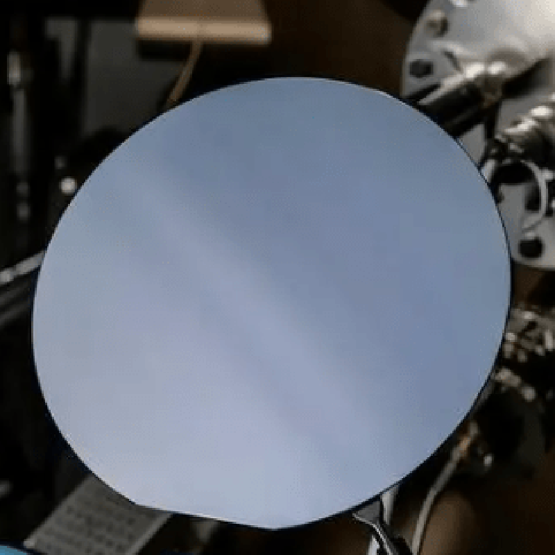
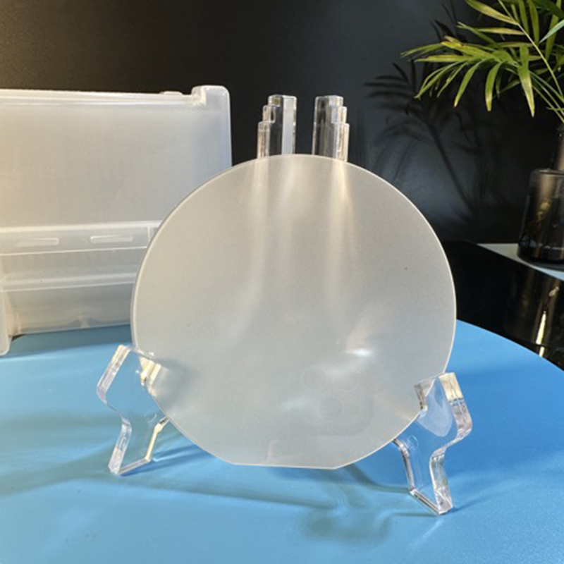
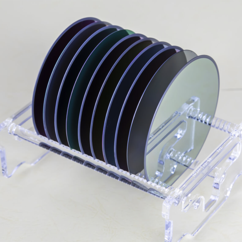
1. Rf power amplifier 2. LED lighting industry 3. Wireless network communication equipment 4. Electronic devices in high temperature environment 5. Optoelectronic devices- Size: The substrate diameter is 6 inches (about 150 mm). - Surface quality: The surface has been finely polished to provide excellent mirror quality. - Thickness: The thickness of GaN layer can be customized according to specific requirements. - Packaging: The substrate is carefully packed with anti-static materials to prevent damage during transportation. - Positioning edges: The substrate has specific positioning edges that facilitate alignment and operation during device preparation. - Other parameters: Specific parameters such as thinness, resistivity and doping concentration can be adjusted according to customer requirements. With their superior material properties and diverse applications, 6-inch sapphire substrate wafers are a reliable choice for the development of high-performance semiconductor devices in various industries.
 | Substrate | 6” 1mm <111> p-type Si | 6” 1mm <111> p-type Si |
| Epi ThickAvg | ~5um | ~7um |
| Epi ThickUnif | <2% | <2% |
| Bow | +/-45um | +/-45um |
| Cracking | <5mm | <5mm |
| Vertical BV | >1000V | >1400V |
| HEMT Al% | 25-35% | 25-35% |
| HEMT ThickAvg | 20-30nm | 20-30nm |
| Insitu SiN Cap | 5-60nm | 5-60nm |
| 2DEG conc. | ~1013cm-2 | ~1013cm-2 |
| Mobility | ~2000cm2/Vs (<2%) | ~2000cm2/Vs (<2%) |
| Rsh | <330ohm/sq (<2%) | <330ohm/sq (<2%) |