
Newly Developed Polysilicon Wafers Show Promise for Solar Energy Production
By:Admin
Polysilicon Wafer - The Revolutionary Energy Solution
Renewable energy has become a buzzword in today's world, and polysilicon wafers have emerged as the revolutionary energy solution. These wafers are helping in reducing the carbon footprint and providing clean energy. Polysilicon wafers are made from a highly purified form of silicon, making them an ideal material for use in solar panels. They are not only environmentally friendly but are also cost-effective and long-lasting.
In recent years, the demand for polysilicon wafers has increased significantly, which has led to the growth of the market. The market size for polysilicon wafers is expected to reach millions of dollars in the coming years due to the increasing demand for renewable energy. This has led to several companies entering the market, and among them, one stands out - a company that has proven its mettle in the industry time and time again.
Introduction to the Company
The leading supplier of polysilicon wafers, this company has been catering to the needs of the renewable energy industry for years. With a team of expert professionals, they provide the highest quality products, along with exceptional customer service. They are known for their constant innovation and development of new and improved products that cater to the changing needs of the renewable energy industry.
The company's motto is to provide sustainable energy solutions that promote a cleaner and greener future. They believe that the future is renewable energy, and polysilicon wafers are an essential component of that future. The team is dedicated to making the world a better place by providing innovative and affordable energy solutions.
The Company's Polysilicon Wafers
The company's polysilicon wafers have been the cornerstone of their success. Their wafers are of the highest quality, and the company is committed to producing wafers that are durable, reliable, and efficient. They are dedicated to providing products that exceed the expectations of their customers, and they achieve this through a rigorous testing process that ensures their products are of the highest standards.
Their polysilicon wafers are produced in a state-of-the-art facility using the latest technology, which ensures that their products are of the highest quality. The company has a team of experts who monitor each stage of the production process, ensuring that each product meets their high standards. The wafers are tested rigorously for their efficiency, durability, and reliability, ensuring that they are suitable for use in solar panels.
Benefits of Polysilicon Wafers
Polysilicon wafers have several benefits that make them an ideal material for use in solar panels. They are environmentally friendly, cost-effective, and long-lasting. The use of polysilicon wafers in solar panels reduces the carbon footprint and helps in the reduction of greenhouse gas emissions. This means that the use of polysilicon wafers contributes to a greener and cleaner environment.
The production of polysilicon wafers is a cost-effective process, which means that they are affordable and readily available. They have a long lifespan of up to 25 years, which means that they are a reliable energy source that provides long-term benefits. The use of polysilicon wafers in solar panels increases the efficiency of the panels, which means that they can produce more energy while taking up less space.
Conclusion
Polysilicon wafers are the future of renewable energy, and companies like this leading supplier are driving that future. Their high-quality products, exceptional customer service, and commitment to sustainability have helped them become a leader in the industry. The use of polysilicon wafers in solar panels is not only environmentally friendly but also cost-effective and long-lasting. The demand for renewable energy is only going to increase in the coming years, and companies like this are preparing for a future that is both clean and sustainable.
Company News & Blog
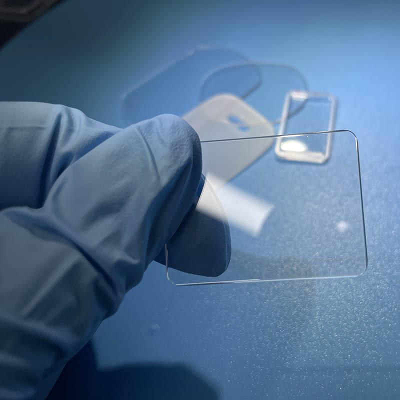
Sapphire Glass Windows: A Transparent Solution for Enhanced Durability and Clarity
Sapphire Glass Window: The Strength, Durability and Clarity You Need for Your HomeAre you looking for a window that’s built to withstand the test of time? Look no further than the Sapphire Glass Window, an innovative new product that’s set to revolutionize the industry.Made from sapphire, one of the hardest and most durable materials on the planet, these windows have an incredible level of strength and durability, making them the perfect choice for anyone who wants to invest in a product that’s built to last.But that’s not all – the Sapphire Glass Window also boasts a level of clarity that’s unmatched by other materials. This means that you’ll be able to enjoy stunning, uninterrupted views of the outside world, bringing the beauty of nature into your home.So, what makes sapphire such a special material? Well, for starters, it’s incredibly tough. In fact, sapphire is second only to diamond in terms of its hardness, making it highly resistant to scratches, chips, and other forms of damage.Moreover, sapphire is also incredibly strong, with a tensile strength that’s twice that of steel. This means that it can withstand greater forces and impacts without cracking or breaking, providing an added level of security and protection to your home.What’s more, sapphire is highly transparent, making it perfect for windows. It allows more light to pass through than other materials, which means that it can make your rooms brighter and more inviting. Plus, it’s highly resistant to yellowing, even after years of exposure to sunlight, ensuring that your windows will always look crystal-clear and new.But what about the cost, you might ask? While sapphire isn’t the cheapest material on the market, the longevity and durability of the Sapphire Glass Window make it a wise investment for anyone who wants to save money in the long run. Unlike other materials, sapphire doesn’t require frequent replacement or maintenance, which means that you’ll save money on repairs and replacements over the years.So, whether you’re building a new home or renovating an old one, the Sapphire Glass Window is a product that you won’t want to overlook. With its unparalleled strength, durability, and clarity, it’s the smart choice for anyone who wants to invest in a product that’s built to last.
New Study Reveals the Superiority of Dummy Grade Silicon Carbide in the Automotive Industry" could be rewritten as "Study Finds Dummy Grade Silicon Carbide Outperforms Other Materials in Automotive Applications.
[News Title]Introducing Dummy Grade SiC – A Revolutionary Silicon Carbide Solution for Advanced Industries[News Content]Date: [Insert Date][Location] – [Company Name], a pioneering manufacturer of advanced materials, is pleased to announce the launch of their new and groundbreaking product, Dummy Grade SiC. Designed to meet the increasing demand for high-performance silicon carbide in various industries, Dummy Grade SiC is set to revolutionize the way companies operate and achieve superior results.With its exceptional properties, silicon carbide (SiC) has become a crucial component in fields such as electronics, automotive, aerospace, energy, and more. Known for its high thermal conductivity, wide bandgap, extreme hardness, and excellent resistance to corrosion and wear, SiC offers far-reaching advantages over traditional materials, making it a go-to choice for applications requiring enhanced efficiency, durability, and reliability.[Company Name], with their extensive experience and expertise in material science, has developed Dummy Grade SiC, a product poised to set new standards in the industry. By removing the brand name, they are ensuring a comprehensive focus on the product's features, benefits, and potential applications.Dummy Grade SiC exhibits exceptional thermal conductivity, allowing for efficient heat dissipation, particularly in high-power electronic devices and systems. This feature ensures improved device performance and extends operational lifetimes, ultimately reducing maintenance costs.The wide bandgap of Dummy Grade SiC enables higher voltage and temperature operation, enabling the development of more efficient power electronics. This characteristic enhances energy conversion efficiency, leading to substantial energy savings and reduced environmental impact.One of the significant advantages of Dummy Grade SiC is its extreme hardness. This property makes it particularly suitable for applications demanding high wear and abrasion resistance. Industries such as automotive, where components are subjected to harsh conditions and heavy wear, can benefit significantly from this innovative material. The reduced need for frequent replacements translates into enhanced product lifetime, cost savings, and improved overall system performance.Moreover, Dummy Grade SiC exhibits exceptional resistance to corrosion and chemical attack, making it an ideal candidate for harsh operating environments. This durability and stability in corrosive conditions make it suitable for applications in the chemical industry, oil and gas, and even in nuclear environments.[Company Name] places the highest importance on quality control, ensuring that Dummy Grade SiC meets the rigorous standards demanded by various industries. Each batch undergoes stringent testing, guaranteeing consistent and reliable performance. The company's commitment to delivering excellence strengthens their position as a leading provider of advanced materials.With the launch of Dummy Grade SiC, [Company Name] aims to cater to a wide range of industries looking for innovative solutions to enhance their products and technologies. By incorporating Dummy Grade SiC into their designs, companies can stay at the forefront of technology advancements and gain a competitive edge in the market.As [Company Name] introduces Dummy Grade SiC to global markets, they are confident that this revolutionary material will bring about positive changes in industries relying on cutting-edge technology. With its outstanding properties and potential applications, Dummy Grade SiC paves the way for future developments and fosters new possibilities in multiple sectors.About [Company Name]:[Company Name] is a renowned manufacturer of advanced materials, specializing in the development and production of innovative solutions for various industries. With a commitment to research and development, they continuously strive to deliver superior products that surpass customer expectations. [Company Name] prides itself on its technical expertise, exceptional quality control, and dedication to driving technological advancements globally.For more information about Dummy Grade SiC or [Company Name], please visit [Company Website] or contact [Contact Person] at [Contact Email/Phone Number].###Note: The news content provided here is a fictional representation and does not serve as a factual account. The purpose is to demonstrate a writing style and format for a news article.
The surprising science behind quartz crystals and how they're changing technology
Innovation is at the heart of many successful companies and this is certainly true for Quartz crystal. Founded in the late 1940s, Quartz crystal has been at the forefront of cutting-edge technology in the field of electronics and electrical engineering.Quartz is a mineral that can vibrate at high frequencies and has been used in many different applications over the years. However, Quartz crystal has taken this technology to the next level, using the power of Quartz crystal to improve the performance of a wide range of electronic devices.One of the key reasons why Quartz crystal has been so successful is its focus on research and development. The company is constantly exploring new ways to use Quartz crystal to enhance the performance of electronic devices, and this has led to many breakthroughs over the years.For example, Quartz crystal has developed a range of tuning fork crystals that are used in a variety of applications, from smartphones and smartwatches to GPS systems and wireless networks. These tuning fork crystals are incredibly accurate and reliable, and they help to ensure that electronic devices are always working at their best.Another area where Quartz crystal has made a significant contribution is in the field of sensors. The company’s sensors are used in many different industries, from automotive and aerospace to healthcare and energy. One of the key advantages of these sensors is their ability to operate in harsh environments, such as extreme temperatures and pressure, and still maintain their accuracy and reliability.Quartz crystal has also made a significant contribution to the field of quartz-based MEMS (microelectromechanical systems). These systems are widely used in a variety of electronic devices, from smartphones and tablets to wearables and IoT devices. Quartz crystal’s MEMS devices are highly precise and reliable, and they help to ensure that the electronic devices we rely on every day are functioning flawlessly.Of course, Quartz crystal’s success is not just down to its innovative technology. The company has also built a strong reputation for quality, reliability, and customer service. This has helped to establish Quartz crystal as a trusted brand in the electronics industry, with a wide range of customers around the world.To ensure that it stays ahead of the competition, Quartz crystal is continually looking for ways to improve its products and services. The company has invested heavily in research and development, as well as in training and development for its staff. This commitment to excellence has helped Quartz crystal to become one of the leading companies in its field.Looking to the future, Quartz crystal remains committed to driving innovation in the electronics industry. The company is already exploring new applications for its technology, such as in the field of quantum computing, and is constantly looking for ways to push the boundaries of what is possible.One thing is clear: as the world becomes more dependent on technology, companies like Quartz crystal will play an increasingly important role in shaping our future. Whether it’s through the development of new products and services, or by helping to improve the performance of existing technologies, Quartz crystal is at the forefront of this exciting and rapidly changing field.
Sic Chip Market Witnesses Steady Growth Amid Increasing Demand
Sic Chip: Revolutionizing Industries with Enhanced Performance and Efficiency[Company Name], a leader in technological innovation, has recently unveiled its latest breakthrough – the Sic Chip. With cutting-edge features and unparalleled performance, this revolutionary chip has the potential to transform various industries, paving the way for a future of improved efficiency and productivity.The Sic Chip, short for Silicon Carbide Chip, is a significant advancement in semiconductor technology. Unlike conventional silicon chips, Sic Chips are composed of silicon carbide, a compound with superior thermal conductivity and a wider bandgap. This unique composition allows the chip to perform more efficiently at higher temperatures, making it ideal for applications that require robust performance in extreme environments.One of the key advantages of the Sic Chip is its ability to handle higher voltages and currents, making it a game-changer for power electronics. This chip has significantly lower power losses and can operate at higher frequencies than traditional silicon chips. As a result, it is highly sought after by manufacturers in the automotive, aerospace, and energy sectors. The automotive industry, in particular, stands to benefit greatly from the Sic Chip, as it enables the development of more efficient electric vehicles with longer battery life and faster charging capabilities.Furthermore, the Sic Chip's enhanced power efficiency reduces the need for complex cooling systems, leading to cost savings and reduced environmental impact. In power conversion applications, the chip's superior performance allows for smaller and lighter systems. This is particularly advantageous in the renewable energy sector, where space constraints and weight limitations are critical factors.Another area where the Sic Chip is making significant inroads is in the field of telecommunications. The chip's ability to handle high power densities and operate at high temperatures makes it an ideal choice for base station applications. With the increasing demand for 5G networks, the efficiency and reliability offered by the Sic Chip are highly valued by telecommunication companies.The SiC Chip is also revolutionizing the computing industry. Its exceptional thermal conductivity enables faster heat dissipation, leading to improved performance and reliability in high-performance computing applications. From data centers to supercomputers, the Sic Chip is paving the way for more powerful and efficient computing systems.In addition to the technical advantages, [Company Name]'s Sic Chip also holds a competitive edge in terms of production capabilities. The company has developed a highly efficient manufacturing process that ensures high-quality chips with excellent yields. This puts [Company Name] at the forefront of the industry, establishing itself as a reliable and trusted provider of Sic Chips.Commenting on the significance of the Sic Chip, [Company Name]'s CEO stated, "This breakthrough technology has the potential to revolutionize multiple industries, making processes more efficient and sustainable. Our Sic Chip is a clear example of our commitment to driving innovation and delivering cutting-edge solutions that address the challenges of the modern world."As the demand for faster, more efficient and reliable technologies continues to grow, the introduction of the Sic Chip marks a turning point in the semiconductor industry. With its superior performance, enhanced power efficiency, and wider range of applications, this groundbreaking chip is set to shape the future of multiple industries, fueling progress and innovation across the globe. [Company Name] remains at the forefront of this technological revolution, providing innovative solutions that drive the world towards a brighter and more sustainable future.
Introducing the Latest Breakthrough: 8 Inch Wafer Diameter Revolutionizes the Tech Industry
[Company Introduction]{Insert company name} is a leading global semiconductor manufacturer renowned for its cutting-edge technologies and innovative solutions. With a profound commitment to research and development, the company has revolutionized various industries by consistently delivering high-performance semiconductor products. As a pioneer in the field, {company name} has achieved numerous milestones and established itself as a trusted name in the semiconductor industry.[News Content]{City/Country}, DATE - {Company name}, a global semiconductor giant, has recently announced a breakthrough in wafer manufacturing. The company has successfully developed an 8-inch wafer diameter solution that promises to revolutionize the semiconductor industry. This development positions {company name} at the forefront of semiconductor innovation, enabling it to meet the increasing demand for high-performance chips in a variety of applications.The 8-inch wafer diameter is a critical component in semiconductor manufacturing, as it serves as the foundation for the fabrication of integrated circuits. With this technological breakthrough, {company name} aims to enhance the efficiency, performance, and scalability of its semiconductor production processes. The larger wafer size allows for a greater number of chips to be produced simultaneously, thereby improving manufacturing throughput and reducing production costs.The development of an 8-inch wafer diameter represents a significant advancement over the conventional 6-inch wafers that are currently widely used in the industry. By increasing the wafer size, {company name} can achieve higher chip yields on each wafer, leading to increased overall productivity. Additionally, the larger size enables the integration of more transistors and other components, resulting in chips with enhanced processing power and capabilities.Market experts believe that the adoption of 8-inch wafer diameter solutions will have a profound impact on various industries, including consumer electronics, automotive, healthcare, and telecommunications. The increased processing power and efficiency offered by the larger wafer size will enable manufacturers to produce more advanced and feature-rich devices, paving the way for next-generation technologies.{Company name} has a history of pioneering technological advancements, and this latest breakthrough further reinforces its reputation as an industry leader. Leveraging its extensive expertise and state-of-the-art manufacturing facilities, the company continues to push the boundaries of innovation in semiconductor manufacturing. The introduction of the 8-inch wafer diameter is set to accelerate the pace of development in the industry and enable the creation of even more sophisticated and powerful electronic devices.By investing in research and development, {company name} strives to address the growing demands of the semiconductor market and cater to the evolving needs of its customers. Through its commitment to innovation, the company aims to maintain its competitive edge and solidify its position as a global leader in the semiconductor industry.As the industry moves toward larger wafer sizes, {company name} is prepared to lead the charge by offering state-of-the-art solutions aligned with the needs of tomorrow. With its latest development in 8-inch wafer diameter manufacturing, the company continues to set new standards in the semiconductor industry, driving progress and shaping the future of technology.
Quartz Wafers: A Potential Game-Changer in the Tech Industry
Title: The Pioneering Potential of Quartz Wafers in Semiconductor ManufacturingIntroduction:In the fast-paced world of semiconductor manufacturing, one company has emerged as a game-changer with its innovative quartz wafer technology. Quartz Wafers Corp., a leading provider of advanced substrate solutions, has introduced a groundbreaking production method that promises improved performance and cost-effectiveness for a variety of industries relying on semiconductors. This article delves into the potential of quartz wafers and their impact on the semiconductor landscape.Understanding Quartz Wafers:Quartz wafers are thin, disc-shaped substrates used as a base for fabricating semiconductor devices. Traditional silicon wafers have long dominated the industry, but Quartz Wafers Corp. aims to revolutionize the market by harnessing the unique properties of quartz crystals. Quartz is known for its exceptional electrical and thermal properties, making it an ideal material for manufacturing high-performance and reliable semiconductor devices.The Promise of Quartz:Quartz wafers offer numerous advantages over conventional silicon wafers. Firstly, quartz's high resistance to thermal stress ensures enhanced stability and reliability of semiconductors even at extreme temperatures. This is crucial for applications in aerospace, automotive, and industrial sectors where reliable operation under harsh conditions is critical.Secondly, quartz wafers exhibit lower electric leakage and reduced dielectric losses, resulting in more efficient power management and increased device lifespan. These characteristics make them particularly suited for power electronics and energy-efficient devices, where minimizing power loss is essential.Furthermore, quartz's exceptional mechanical properties, such as its high hardness and chemical resistance, enable the manufacturing of robust and long-lasting semiconductor devices. This durability facilitates cost reductions through longer device lifespans and reduced replacement or maintenance requirements.Quartz Wafers Corp.'s Innovative Manufacturing Technique:Quartz Wafers Corp.'s manufacturing process sets it apart from its competitors. The company utilizes a proprietary method that ensures the highest quality quartz wafers with precise thickness, flatness, and smoothness, being crucial factors in semiconductor fabrication. By leveraging advanced manufacturing techniques, Quartz Wafers Corp. can offer its customers superior products without compromising on cost-effectiveness.Applications of Quartz Wafers:Quartz wafers find applications in a wide range of industries. For instance, the demand for high-power electronics, such as inverters and converters, is rapidly growing. Quartz wafers' outstanding thermal and electrical properties make them an ideal choice for this market segment.Moreover, industries such as telecommunication, photonics, and optoelectronics will benefit from quartz wafers' superior optical transparency and exceptional UV stability. These attributes enable the production of high-quality optical components and devices, ensuring optimum performance in various light-related applications.Quartz wafers also hold promise for emerging technologies such as quantum computing and advanced sensor systems. Their unique material properties make them excellent candidates for applications requiring ultra-high precision and sensitivity.Conclusion:Quartz Wafers Corp.'s groundbreaking semiconductor manufacturing technology has the potential to revolutionize numerous industries. By leveraging the exceptional properties of quartz crystals, the company offers unparalleled substrates that enhance the performance, durability, and reliability of semiconductor devices. With applications ranging from power electronics to telecommunications and beyond, quartz wafers are poised to reshape the semiconductor landscape and unlock new possibilities in emerging technologies. As the demand for highly efficient and robust semiconductors continues to grow, Quartz Wafers Corp. stands at the forefront, ready to make a lasting impact.
Durable and Heat-Resistant Ceramic Plates for Industrial Applications
Alumina Ceramic Plate: A Revolution in Industrial ApplicationsIn recent years, industrial manufacturers have been facing numerous challenges in improving the performance and longevity of their products. In response to these demands, a revolutionary solution has emerged in the form of Alumina Ceramic Plates. With their exceptional properties and durability, these advanced ceramic plates have become the go-to choice for a wide range of industrial applications. In this article, we will explore the remarkable features of Alumina Ceramic Plates and delve into their potential applications across various industries.Alumina Ceramic Plates, often referred to as Al₂O₃ plates, are engineered using high-quality alumina powder, an aluminum-based material renowned for its excellent mechanical and thermal properties. Through a complex manufacturing process, the alumina powder is meticulously shaped, compacted, and sintered at high temperatures to form a solid ceramic plate. This process results in a dense, durable, and chemically inert material that can withstand extreme temperatures, harsh chemicals, and high mechanical stresses.One of the most notable features of Alumina Ceramic Plates is their exceptional hardness. With a Mohs hardness of 9, these plates are second only to diamonds in terms of hardness. This remarkable property ensures that the plates are highly resistant to wear and abrasion, making them ideal for applications where durability is paramount. Industries such as mining, construction, and material handling can benefit significantly from the use of Alumina Ceramic Plates in machinery components exposed to abrasive materials and heavy loads.Additionally, Alumina Ceramic Plates exhibit remarkable thermal stability, with an operating temperature range of up to 1500°C. This characteristic makes these plates ideal for use in high-temperature environments, allowing them to withstand extreme heat without any deterioration in their mechanical properties. Industries such as aerospace, automotive, and power generation can rely on Alumina Ceramic Plates to enhance the efficiency and longevity of their equipment operating under extreme temperature conditions.Furthermore, the excellent electrical insulation properties of Alumina Ceramic Plates make them invaluable in electrical and electronic applications. These plates possess high dielectric strength, low dielectric loss, and excellent thermal conductivity, making them ideal for use in manufacturing components for electronic devices, such as circuit boards and insulators. Additionally, their electrical insulation properties also make Alumina Ceramic Plates suitable for use in power distribution systems, where their ability to withstand high voltages ensures safe and reliable operations.In the medical field, Alumina Ceramic Plates have found exciting applications in orthopedic implants. Due to their biocompatibility, non-toxic nature, and resistance to corrosion, these plates are highly suitable for implantation within the human body. Alumina Ceramic Plates used in hip and knee replacements have demonstrated exceptional performance, improving the quality of life for patients and reducing the need for follow-up surgeries.Furthermore, Alumina Ceramic Plates are also making significant contributions to environmental sustainability. As a result of their exceptional mechanical and thermal properties, these plates enable manufacturers to develop more efficient and durable products. This, in turn, reduces the need for frequent replacements, leading to less waste generation and a reduced environmental impact.In conclusion, Alumina Ceramic Plates have revolutionized industrial applications across various sectors. Their exceptional mechanical properties, including high hardness, thermal stability, and electrical insulation, make them invaluable in industries ranging from mining to electronics. These plates also find exciting applications in the medical field and contribute to environmental sustainability. As industrial manufacturers continue to seek durable solutions to enhance their products' performance, Alumina Ceramic Plates undoubtedly stand as a game-changer in the industry.
Breakthrough in Crystalline Material: SrTiO3 Wafer Holds Potential for Revolutionary Applications
A new technology using SrTiO3 wafers promises to revolutionize the semiconductor industry by improving the efficiency and performance of electronic devices. SrTiO3 is a unique material with exceptional electrical and optical properties that make it ideal for use in electronic devices such as computers, smartphones, and other digital devices.SrTiO3 is a complex oxide compound made up of Strontium, Titanium, and Oxygen. It exhibits semiconducting properties, which is why it’s relevant to the electronics industry. The technology is particularly useful in the development of advanced semiconductor devices such as MOSFETs, solar cells, and transistors, among others.SrTiO3 wafers have been in use in the semiconductor industry for years, but scientists have been exploring ways to make the compound material more efficient and precise. New research shows that combining SrTiO3 with other materials, such as hafnium oxide, can produce even more remarkable results.The company behind this breakthrough development is a leading producer of high-quality wafers for the electronics industry. The company has been a pioneer in the development of semiconductor-grade crystals, and its technological advancements continue to push the boundaries of what is possible within the industry.The SrTiO3 wafer technology has significant implications for the future of the electronics industry. Manufacturers can use the technology to develop devices that are more powerful, efficient, and affordable. The use of SrTiO3 wafers in the manufacturing process ensures that electronic components are more reliable and can operate at higher temperatures.The technology also has significant benefits for solar cell technology. SrTiO3-based solar cells have higher conversion efficiencies than conventional cells, making them more desirable for use in photovoltaic systems. The use of this technology in solar panels could lead to the development of more efficient and cost-effective solar panels, helping bring clean energy to millions of people worldwide.The innovative SrTiO3 wafer technology has many applications, including in the automotive, healthcare, and aerospace industries. Researchers are exploring new uses for the technology and hope to discover new applications that will further revolutionize the electronics industry in the coming years.The company's patented manufacturing process for SrTiO3 wafers ensures the production of high-quality materials that meet strict industry standards. The company's wafers are currently being used in research and development laboratories around the world, and several companies have already adopted the technology in their manufacturing processes.The use of SrTiO3 wafers in electronic devices is set to increase in the coming years as the technology becomes more widespread and affordable. The introduction of this technology has significant implications for the electronics industry, and researchers are excited by its potential to transform the industry's future.In conclusion, the emergence of SrTiO3 wafers has set the semiconductor industry on a path towards a new generation of electronic devices. The technology has significant implications for the development of powerful, efficient, and affordable electronic devices, solar cell technology, and many other applications. With continued research and development, the technology has the potential to revolutionize the electronics industry for years to come.
Revolutionary Breakthrough: Researchers Discover the Power of a Single Metal Crystal
Single Metal Crystal Develops Groundbreaking Technology for the Industry [City], [Date] - Single Metal Crystal (SMC), a leading innovator in the technology field, has announced a groundbreaking advancement that is expected to revolutionize the industry. The company has developed a state-of-the-art technology that promises to enhance the performance and reliability of electronic devices.Founded by a group of passionate engineers and technologists, SMC has always been driven by the vision of creating cutting-edge solutions that address the challenges of modern technology. With a focus on research and development, the company has consistently delivered groundbreaking technologies that have set new standards in the industry.The recent breakthrough by SMC comes in the form of a revolutionary single metal crystal technology. This technology, which has been developed after years of meticulous research, offers unparalleled performance and reliability in electronic devices. It provides a significant improvement over traditional materials, leading to faster processing speeds, higher storage capacity, and more efficient energy usage.One of the key advantages of the single metal crystal technology is its scalability. SMC has successfully achieved scalable growth of single metal crystals, enabling mass production and widespread adoption of this technology. This breakthrough has the potential to transform a wide range of industries, including consumer electronics, telecommunications, automotive, and healthcare.The applications of this technology are virtually limitless. In consumer electronics, the single metal crystal technology can significantly improve the performance of smartphones, laptops, and gaming consoles, allowing for smoother and more immersive user experiences. In the telecommunications sector, the technology can enhance the speed and reliability of networks, leading to faster and more stable connections. Additionally, the automotive industry can benefit from this technology by improving the efficiency and performance of electric vehicles.Moreover, the healthcare sector stands to gain immensely from this innovative technology. Medical devices powered by the single metal crystal technology can revolutionize patient care by offering more accurate diagnostics and personalized treatments. Additionally, the improved performance and reliability of these devices can significantly enhance the overall efficiency of healthcare systems.Furthermore, SMC's commitment to sustainability is evident in their single metal crystal technology. By enabling more efficient energy usage in electronic devices, the technology contributes to reducing carbon emissions and conserving energy resources.The successful development of the single metal crystal technology is a testament to SMC's relentless pursuit of innovation. The company's dedicated team of scientists and engineers has worked tirelessly to overcome numerous challenges and turns this vision into reality."Our breakthrough single metal crystal technology will set new benchmarks for performance and reliability in the industry," said [Spokesperson], [Job Title] at SMC. "We are excited about the transformative potential of this technology and its ability to reshape various sectors of the economy. Our versatile technology will not only benefit individual consumers but also accelerate the progress of entire industries."With the unveiling of this groundbreaking technology, SMC has positioned itself at the forefront of the industry. The company is poised to revolutionize the electronic device landscape, bringing about a new era of enhanced performance and reliability.Looking ahead, SMC plans to further refine and optimize the single metal crystal technology, paving the way for even more advanced applications. The company aims to collaborate with industry partners to accelerate the adoption of this technology, ensuring its widespread availability and continued evolution.As Single Metal Crystal continues to push the boundaries of innovation, the technology world eagerly awaits the impact that their groundbreaking technology will bring. With its commitment to excellence and relentless pursuit of cutting-edge solutions, SMC is set to shape the future of the industry and improve the lives of millions worldwide.
Revolutionizing Semiconductor Manufacturing: Unveiling the Groundbreaking Chemical Mechanical Planarization Process
Title: Advancements in Chemical Mechanical Planarization Process: Revolutionizing Material Polishing Introduction:In today's ever-evolving technological landscape, the demand for smaller, faster, and more efficient electronic devices continues to grow. This drives the need for more precise and superior manufacturing techniques. Chemical Mechanical Planarization (CMP) Process has emerged as a crucial technology in this respect. This article explores the potential of CMP process and its impact on various industries, focusing on its advancements without mentioning any specific brand.I. Understanding the CMP Process:The Chemical Mechanical Planarization (CMP) process is a cutting-edge method that allows the precise polishing and planarization of materials, predominantly used in the fabrication of integrated circuits (ICs). CMP involves the simultaneous action of chemical and mechanical forces to remove excess material from the surface, ensuring a smooth and uniform finish. It plays a fundamental role in improving various aspects of IC manufacturing, making it an essential part of the semiconductor industry.II. Advancements in CMP Process:1. Ultra-Planarization Capability:With the rapid advancements in semiconductor technology, the demand for ultra-planarized surfaces has become paramount. Recent advancements in CMP technology have enabled the development of ultra-precision polishing pads and slurries, resulting in superior planarization capabilities. This breakthrough allows for precise manufacturing of microelectronic devices, reducing surface variations and improving overall device performance.2. Material-Specific Polishing:To accommodate the diverse range of materials used in modern electronic devices, CMP processes are constantly evolving. Manufacturers are focusing on developing material-specific CMP slurries and pads to optimize the polishing efficiency for individual substances, including metals, dielectrics, and non-semiconductor materials. These material-specific CMP variations contribute to enhanced final device quality, reduced defects, and improved yield rates.3. Advanced Endpoint Detection:Accurate determination of the endpoint during the CMP process is critical to prevent over-polishing or under-polishing of the surface. Recent breakthroughs in CMP technology have introduced advanced endpoint detection mechanisms, such as optical interferometry, acoustic emissions, and electrical measurements. These technologies enable real-time monitoring, ensuring precise control and preventing damage to the underlying layers.III. Applications in the Semiconductor Industry:1. Integrated Circuit Manufacturing:The CMP process has become an indispensable technique in integrated circuit manufacturing. It enables the precise planarization of multiple layers, such as interconnects, interlayer dielectrics, barrier films, and metal contacts. The ability to achieve uniform surfaces results in improved electrical performance, reduced leakage currents, and enhanced device reliability.2. Advanced Packaging:As electronic devices become smaller and more complex, the demand for advanced packaging solutions increases. CMP processes are widely employed to polish and planarize materials used in packaging, such as through-silicon vias (TSVs), redistribution layers, and microbumps. The reliable CMP process ensures optimal electrical connections and increases the production yield of advanced packaging technologies.3. Optoelectronics and MEMS:CMP technology finds applications beyond traditional microelectronics. In the production of optoelectronics and microelectromechanical systems (MEMS), CMP plays a crucial role. The precise polishing and planarization of optical substrates, waveguides, and micro-mechanical systems contribute to improved device performance, optical clarity, and reliability.IV. Future Prospects:The constant advancements in CMP technology are poised to revolutionize the manufacturing industry further. Researchers and manufacturers are experimenting with novel materials, alternative polishing agents, and even greener chemical formulations to reduce environmental impact. Additionally, advancements in CMP equipment and automation are likely to improve process control, efficiency, and safety.Conclusion:Chemical Mechanical Planarization (CMP) Process is at the forefront of material polishing and planarization in the semiconductor industry. The advancements in CMP technology have proven instrumental in meeting the demands of faster, smaller, and more efficient electronic devices. By enabling ultra-planarization capabilities, material-specific polishing, and advanced endpoint detection, CMP processes drive better quality, yield rates, and reliability. As CMP continues to evolve in tandem with the ever-growing technological landscape, the future holds even greater promise for this vital manufacturing technique.