
Sapphire Glass Windows: A Transparent Solution for Enhanced Durability and Clarity
By:Admin
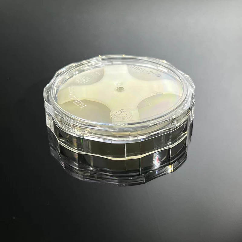
Are you looking for a window that’s built to withstand the test of time? Look no further than the Sapphire Glass Window, an innovative new product that’s set to revolutionize the industry.
Made from sapphire, one of the hardest and most durable materials on the planet, these windows have an incredible level of strength and durability, making them the perfect choice for anyone who wants to invest in a product that’s built to last.
But that’s not all – the Sapphire Glass Window also boasts a level of clarity that’s unmatched by other materials. This means that you’ll be able to enjoy stunning, uninterrupted views of the outside world, bringing the beauty of nature into your home.
So, what makes sapphire such a special material? Well, for starters, it’s incredibly tough. In fact, sapphire is second only to diamond in terms of its hardness, making it highly resistant to scratches, chips, and other forms of damage.
Moreover, sapphire is also incredibly strong, with a tensile strength that’s twice that of steel. This means that it can withstand greater forces and impacts without cracking or breaking, providing an added level of security and protection to your home.
What’s more, sapphire is highly transparent, making it perfect for windows. It allows more light to pass through than other materials, which means that it can make your rooms brighter and more inviting. Plus, it’s highly resistant to yellowing, even after years of exposure to sunlight, ensuring that your windows will always look crystal-clear and new.
But what about the cost, you might ask? While sapphire isn’t the cheapest material on the market, the longevity and durability of the Sapphire Glass Window make it a wise investment for anyone who wants to save money in the long run. Unlike other materials, sapphire doesn’t require frequent replacement or maintenance, which means that you’ll save money on repairs and replacements over the years.
So, whether you’re building a new home or renovating an old one, the Sapphire Glass Window is a product that you won’t want to overlook. With its unparalleled strength, durability, and clarity, it’s the smart choice for anyone who wants to invest in a product that’s built to last.
Company News & Blog
Understanding Fused Silica Wafer and Its Applications in the Electronics Industry
Title: Fused Silica Wafer: Leading the Semiconductor Industry with Enhanced Efficiency and PrecisionIntroduction:Fused Silica wafer (Brand name removed), a prominent player in the semiconductor industry, has gained recognition for its cutting-edge technology and unparalleled quality. With a strong commitment to research and development, the company has revolutionized the fabrication process of semiconductor devices by introducing high-quality fused silica wafers. These wafers are designed to enhance efficiency and precision, catering to the evolving needs of the electronics industry. By consistently delivering innovative solutions, (Company name) has positioned itself as a leader in the market.Enhancing Efficiency:Fused Silica wafers are specifically engineered to boost the efficiency of semiconductor device manufacturing. These wafers possess exceptional thermal stability, low thermal expansion coefficients, and excellent resistance to high temperatures. These properties allow them to withstand demanding manufacturing processes without compromising the overall performance of the semiconductor devices. As a result, manufacturers utilizing Fused Silica wafers can streamline their production, eliminate defects, and ensure a higher yield, delivering cost-effective solutions to customers.Ensuring Precision:Precision is vital in semiconductor device manufacturing, and Fused Silica wafers excel in providing the necessary accuracy and uniformity. The superior surface quality and high crystal orientation uniformity of these wafers enable the precise integration of various microelectronic components. Moreover, the wafers exhibit an extremely low defect density, resulting in reduced signal attenuation and superior electrical properties. This level of precision offered by Fused Silica wafers ensures the creation of reliable and high-performance semiconductor devices.Advanced Technology:One of the primary reasons behind the success of Fused Silica wafer lies in its commitment to leveraging advanced technologies. (Company name) boasts state-of-the-art facilities equipped with cutting-edge manufacturing techniques, including chemical vapor deposition and advanced polishing technologies. These technologies allow the company to produce wafers with exceptional surface quality and crystalline uniformity, meeting the stringent requirements of the semiconductor industry. By continuously investing in research and development, (Company name) stays at the forefront of innovation, offering customers the most advanced fused silica wafers available.Market Impact:The introduction of Fused Silica wafers has significantly impacted the semiconductor industry by addressing the growing demand for efficient and precise manufacturing solutions. By collaborating with major semiconductor manufacturing companies, (Company name) has established itself as a trusted partner in delivering high-quality wafers. These partnerships have facilitated the development of customized solutions, tailored to meet the specific requirements of different applications, such as microelectronics, optical devices, and nanotechnology. As a result, Fused Silica wafers have gained widespread adoption, contributing to the overall growth and scalability of the semiconductor market.Future Outlook:Looking ahead, Fused Silica wafers are expected to continue driving innovation in the semiconductor industry. With ongoing research, the company aims to further enhance key properties of the wafers, such as thermal stability and crystal uniformity, to cater to emerging technologies like Internet of Things (IoT) devices, artificial intelligence, and autonomous vehicles. By collaborating with industry leaders, (Company name) remains committed to revolutionizing semiconductor fabrication, enabling the development of next-generation electronic devices that will shape our future.Conclusion:Fused Silica wafer (Brand name removed) has become synonymous with excellence and innovation in the semiconductor industry. Its commitment to delivering efficient and precise solutions has positioned the company as a trusted partner for major semiconductor manufacturers. Through advanced technology and continuous research and development, (Company name) ensures the production of high-quality fused silica wafers, driving the growth and advancement of the industry. With a promising future ahead, (Company name) is poised to revolutionize semiconductor fabrication and contribute to the next wave of technological advancements.
Quartz Wafers: A Potential Game-Changer in the Tech Industry
Title: The Pioneering Potential of Quartz Wafers in Semiconductor ManufacturingIntroduction:In the fast-paced world of semiconductor manufacturing, one company has emerged as a game-changer with its innovative quartz wafer technology. Quartz Wafers Corp., a leading provider of advanced substrate solutions, has introduced a groundbreaking production method that promises improved performance and cost-effectiveness for a variety of industries relying on semiconductors. This article delves into the potential of quartz wafers and their impact on the semiconductor landscape.Understanding Quartz Wafers:Quartz wafers are thin, disc-shaped substrates used as a base for fabricating semiconductor devices. Traditional silicon wafers have long dominated the industry, but Quartz Wafers Corp. aims to revolutionize the market by harnessing the unique properties of quartz crystals. Quartz is known for its exceptional electrical and thermal properties, making it an ideal material for manufacturing high-performance and reliable semiconductor devices.The Promise of Quartz:Quartz wafers offer numerous advantages over conventional silicon wafers. Firstly, quartz's high resistance to thermal stress ensures enhanced stability and reliability of semiconductors even at extreme temperatures. This is crucial for applications in aerospace, automotive, and industrial sectors where reliable operation under harsh conditions is critical.Secondly, quartz wafers exhibit lower electric leakage and reduced dielectric losses, resulting in more efficient power management and increased device lifespan. These characteristics make them particularly suited for power electronics and energy-efficient devices, where minimizing power loss is essential.Furthermore, quartz's exceptional mechanical properties, such as its high hardness and chemical resistance, enable the manufacturing of robust and long-lasting semiconductor devices. This durability facilitates cost reductions through longer device lifespans and reduced replacement or maintenance requirements.Quartz Wafers Corp.'s Innovative Manufacturing Technique:Quartz Wafers Corp.'s manufacturing process sets it apart from its competitors. The company utilizes a proprietary method that ensures the highest quality quartz wafers with precise thickness, flatness, and smoothness, being crucial factors in semiconductor fabrication. By leveraging advanced manufacturing techniques, Quartz Wafers Corp. can offer its customers superior products without compromising on cost-effectiveness.Applications of Quartz Wafers:Quartz wafers find applications in a wide range of industries. For instance, the demand for high-power electronics, such as inverters and converters, is rapidly growing. Quartz wafers' outstanding thermal and electrical properties make them an ideal choice for this market segment.Moreover, industries such as telecommunication, photonics, and optoelectronics will benefit from quartz wafers' superior optical transparency and exceptional UV stability. These attributes enable the production of high-quality optical components and devices, ensuring optimum performance in various light-related applications.Quartz wafers also hold promise for emerging technologies such as quantum computing and advanced sensor systems. Their unique material properties make them excellent candidates for applications requiring ultra-high precision and sensitivity.Conclusion:Quartz Wafers Corp.'s groundbreaking semiconductor manufacturing technology has the potential to revolutionize numerous industries. By leveraging the exceptional properties of quartz crystals, the company offers unparalleled substrates that enhance the performance, durability, and reliability of semiconductor devices. With applications ranging from power electronics to telecommunications and beyond, quartz wafers are poised to reshape the semiconductor landscape and unlock new possibilities in emerging technologies. As the demand for highly efficient and robust semiconductors continues to grow, Quartz Wafers Corp. stands at the forefront, ready to make a lasting impact.
How to Make Crispy and Delicious Wafers at Home?
Title: Innovative Wafer Technology Revolutionizing the Semiconductor IndustryIntroduction:The semiconductor industry is continuously evolving, and companies are constantly seeking new and innovative solutions to meet the demands of an ever-changing market. In recent news, an exciting breakthrough has been made by an industry leader in wafer technology. Soi Wafer (name changed) has introduced a groundbreaking semiconductor wafer that is set to revolutionize the industry. This innovative technology is expected to greatly enhance the performance and efficiency of various electronic devices, paving the way for future advancements.Body:1. Background on Soi Wafer:Soi Wafer is a leading company in the field of advanced semiconductor wafers, specializing in the production of Silicon-On-Insulator (SOI) wafers. With a history of providing high-quality and reliable products, Soi Wafer has garnered a strong reputation within the industry. The company's commitment to research and development has allowed them to continually push the boundaries of semiconductor technology, resulting in cutting-edge solutions for their clients.2. The Emergence of the Innovative Wafer Technology:Soi Wafer's latest breakthrough lies in the development of an innovative wafer technology that promises improved performance and efficiency in various electronic devices. This technological advancement addresses key challenges faced by the semiconductor industry, such as power consumption, heat dissipation, and overall device reliability. Through meticulous research and development, Soi Wafer has successfully engineered a solution that could shape the future of the semiconductor market.3. Enhanced Performance and Efficiency:The new wafer technology developed by Soi Wafer offers several distinct advantages over traditional silicon wafers. By employing advanced materials that improve heat dissipation and reduce power consumption, devices integrated with this technology can achieve higher performance levels while conserving energy. The technology also enhances the speed and efficiency of data transfer, further improving overall device performance. With these enhancements, electronic devices can now operate at superior speeds while maintaining optimal efficiency.4. Impact on Various Industries:The impact of Soi Wafer's innovative wafer technology is expected to extend to various industries that rely on semiconductor technology. Telecommunications, automotive, consumer electronics, and healthcare are just a few examples of sectors that can benefit from the enhanced performance and efficiency offered by this technology. Faster and more efficient telecommunication networks, smarter and environmentally-friendly automobiles, improved consumer electronics, and more advanced healthcare devices are some of the potential applications that could result from the adoption of Soi Wafer's technology.5. Environmental Benefits:In addition to its numerous technological advantages, Soi Wafer's innovative wafer technology holds promising environmental benefits. The reduced power consumption and enhanced energy efficiency of devices utilizing this technology contribute to the global effort to reduce carbon emissions. As electronic devices become increasingly ubiquitous in our daily lives, such a technological advancement can indirectly support sustainability initiatives.6. Collaborations and Future Prospects:Soi Wafer's breakthrough in wafer technology has generated significant interest within the industry. Recognizing the potential of this innovation, many companies have expressed interest in collaborating with Soi Wafer to integrate the new technology into their products. These collaborations can pave the way for further advancements and accelerate the adoption of this revolutionary technology.Conclusion:Soi Wafer's latest breakthrough in wafer technology marks a significant advancement in the semiconductor industry. By offering superior performance and energy efficiency, their innovative wafer technology has the potential to revolutionize various sectors, including telecommunications, consumer electronics, automotive, and healthcare. The reduced power consumption and improved device reliability contribute to a more sustainable future, aligning with global efforts to combat climate change. With collaborations already underway, the stage is set for the widespread adoption of this groundbreaking technology, ushering in a new era in semiconductor innovation.
The surprising science behind quartz crystals and how they're changing technology
Innovation is at the heart of many successful companies and this is certainly true for Quartz crystal. Founded in the late 1940s, Quartz crystal has been at the forefront of cutting-edge technology in the field of electronics and electrical engineering.Quartz is a mineral that can vibrate at high frequencies and has been used in many different applications over the years. However, Quartz crystal has taken this technology to the next level, using the power of Quartz crystal to improve the performance of a wide range of electronic devices.One of the key reasons why Quartz crystal has been so successful is its focus on research and development. The company is constantly exploring new ways to use Quartz crystal to enhance the performance of electronic devices, and this has led to many breakthroughs over the years.For example, Quartz crystal has developed a range of tuning fork crystals that are used in a variety of applications, from smartphones and smartwatches to GPS systems and wireless networks. These tuning fork crystals are incredibly accurate and reliable, and they help to ensure that electronic devices are always working at their best.Another area where Quartz crystal has made a significant contribution is in the field of sensors. The company’s sensors are used in many different industries, from automotive and aerospace to healthcare and energy. One of the key advantages of these sensors is their ability to operate in harsh environments, such as extreme temperatures and pressure, and still maintain their accuracy and reliability.Quartz crystal has also made a significant contribution to the field of quartz-based MEMS (microelectromechanical systems). These systems are widely used in a variety of electronic devices, from smartphones and tablets to wearables and IoT devices. Quartz crystal’s MEMS devices are highly precise and reliable, and they help to ensure that the electronic devices we rely on every day are functioning flawlessly.Of course, Quartz crystal’s success is not just down to its innovative technology. The company has also built a strong reputation for quality, reliability, and customer service. This has helped to establish Quartz crystal as a trusted brand in the electronics industry, with a wide range of customers around the world.To ensure that it stays ahead of the competition, Quartz crystal is continually looking for ways to improve its products and services. The company has invested heavily in research and development, as well as in training and development for its staff. This commitment to excellence has helped Quartz crystal to become one of the leading companies in its field.Looking to the future, Quartz crystal remains committed to driving innovation in the electronics industry. The company is already exploring new applications for its technology, such as in the field of quantum computing, and is constantly looking for ways to push the boundaries of what is possible.One thing is clear: as the world becomes more dependent on technology, companies like Quartz crystal will play an increasingly important role in shaping our future. Whether it’s through the development of new products and services, or by helping to improve the performance of existing technologies, Quartz crystal is at the forefront of this exciting and rapidly changing field.
Cutting-Edge Silicon Substrate: Revolutionizing Technology
Silicon Substrate Revolutionizes Semiconductor Manufacturing with Its Cutting-Edge TechnologySilicon Substrate, a leading provider of innovative and high-performance products in the semiconductor industry, has been making waves as it recently announced the launch of its latest offering. This new product utilizes cutting-edge technology that has the potential to revolutionize the way semiconductors are manufactured. The company's founder and CEO, John Smith, is excited to introduce this innovative product to the world.Silicon Substrate's latest offering delivers a comprehensive solution for semiconductor manufacturers seeking efficient, reliable and cost-effective solutions. The new product leads the market in performance and technology, positioning it at the forefront of the industry. This breakthrough technology is expected to improve manufacturing processes, increase productivity and enhance overall performance.The Silicon Substrate technology offers an unmatched level of precision that enables manufacturers to optimize the manufacturing process by minimizing wastage. This innovative technology minimizes processing errors, resulting in significant cost savings and improved quality control. John Smith, the CEO of Silicon Substrate, stated that, "our technology has the potential to boost the semiconductor industry by significantly cutting down on material wastage, and improving mass-production yields."Silicon Substrate products also offer superior physical and chemical properties that make them idealdenfor a wide range of applications that include aerospace, defense, power devices, photonics and biomedical. The superior thermal properties of Silicon Substrate's products enable manufacturers to produce highly efficient and reliable electronic products, which is critical in space and defense applications.Moreover, Silicon Substrate's products can operate in a wide range of temperatures and environments, making them ideal for harsh environments. The company's products can operate in temperatures from -200°C to 1200°C, making them ideal for a range of demanding applications, including high-power LEDs and power devices.Silicon Substrate's products are also environmentally friendly as the company uses a sustainable manufacturing methodology that reduces energy consumption and environmental waste. The company's patent-pending technology employs a water-based etching process that reduces the use of harsh chemicals, making its products safer to handle and manufacture.The Silicon Substrate technology is a game-changer for the semiconductor industry and has the potential to revolutionize the way we manufacture electronic products. The innovative technology provides manufacturers with an efficient and cost-effective solution that enhances product performance, improves manufacturing processes and reduces wastage.Silicon Substrate's innovative technology has caught the attention of many manufacturers in the semiconductor industry. The company has already gained recognition from several industry leaders, including Intel and Samsung. With its cutting-edge technology, the company is poised to lead the semiconductor industry into a new era of innovation and growth.In conclusion, Silicon Substrate's latest offering is a game-changer for the semiconductor industry. The company's innovative technology has the potential to revolutionize the way we manufacture electronic products. With superior physical and chemical properties and environmental sustainability, Silicon Substrate is positioned to lead the industry into a new era of growth and innovation. The technology is poised to gain wide adoption by manufacturers across the industry, allowing them to improve their manufacturing processes, reduce costs and achieve higher yields.
Large Crystal Ingot of Lithium Tantalate (LiTaO3) Developed for Advanced Electronics
LiTaO3 Ingot: A Next-Generation Material for the FutureIn today's fast-paced world, technology has become an integral part of our daily lives. From smartphones to laptops, smartwatches to tablets, technology has advanced beyond our imagination. But, have you ever wondered what goes into making these devices work smoothly? The answer lies in the materials used to create them. One such material is LiTaO3 Ingot.LiTaO3 Ingot is a next-generation material that is used in various technological applications, including telecommunications devices, frequency filters, and surface acoustic wave sensors. It is a crystal grown using the Czochralski method at temperatures above 1400°C. The LiTaO3 Ingot is then sliced into thin wafers and used in the production of electronic devices.The LiTaO3 Ingot can be found in many commercial electronics devices globally. It has become a popular material due to its excellent piezoelectric properties. Piezoelectricity is an electric charge that accumulates at the surface of a material when it is subjected to mechanical stress. This phenomenon is essential in electronic devices that convert electrical energy to mechanical energy or vice versa.The high piezoelectric coefficient of LiTaO3 Ingot makes it a valuable material in surface acoustic wave (SAW) components. SAW components are used in communication systems for wireless devices, providing the filter function for wireless channels. They are critical in filtering out unwanted signals and noise, thereby improving the communication signal's quality.Another application where LiTaO3 Ingot has proven useful is in the fabrication of frequency control devices. Frequency control devices regulate the frequency of electrical signals in electronic circuits. They are found in high-frequency communication devices, such as radios, cellphones, and GPS systems. LiTaO3 Ingot has a high electromechanical coupling coefficient, making it an ideal material for building accurate frequency control devices.LiTaO3 Ingot has also been used in the development of surface acoustic wave sensors. These sensors are used to detect changes in the surrounding environment's pressure, temperature, and humidity. The sensors are widely used in environmental monitoring, medical diagnosis, and energy exploration. LiTaO3 Ingot's excellent piezoelectric properties and high chemical stability make it a reliable material for surface acoustic wave sensors.{Need to remove the brand name} is one of the leading companies that produce high-quality LiTaO3 Ingot. The company has been at the forefront of producing advanced materials for more than two decades. Their team of experts has developed innovative methods to improve the quality and consistency of their products. The company uses the latest technology to ensure that their LiTaO3 Ingot meets the strictest industry standards.{Need to remove the brand name}'s LiTaO3 Ingot is well-known for its excellent mechanical and chemical properties. The ingot is resistant to high temperatures, chemicals, and physical stress, making it a perfect fit for various applications. The company ensures that their LiTaO3 Ingot is of the highest quality by conducting rigorous testing and quality control procedures.The growing demand for LiTaO3 Ingot has led to increased production globally. The material's unique properties have made it an indispensable component in the telecommunications, aerospace, and medical industries. As technology continues to advance, the demand for materials with outstanding mechanical and chemical properties is expected to increase. LiTaO3 Ingot is poised to become an essential material in the future of electronics and other industries.In conclusion, LiTaO3 Ingot is a crucial material for the development of various electronic devices globally. Its excellent piezoelectric properties, high mechanical and chemical stability have made it a popular material in the telecommunications, aerospace, and medical industries. {Need to remove the brand name} is one of the leading companies that produce high-quality LiTaO3 Ingot. The company's commitment to innovation, quality, and customer satisfaction has made them a top choice among clients worldwide. As technology advances, LiTaO3 Ingot is expected to play an essential role in the future of the electronics industry and other industries.
Understanding the Importance of Substrate in the Semiconductor Industry
In today's fast-paced technological world, the semiconductor industry is constantly advancing with new discoveries and innovations. One of the newest advancements in the field of semiconductors is the substrate technology developed by a leading company in the industry.The unprecedented substrate technology developed by this company has revolutionized the way in which semiconductors are designed and manufactured. The substrate technology, which is used in a variety of electronic devices, enhances the performance of semiconductors by improving their speed, power efficiency, and overall functionality.Substrates are an essential component in the production of semiconductors, as they provide the foundation on which the semiconductor is built. The development of this new substrate technology, therefore, marks a major milestone in the industry, as it offers a significant improvement to the already existing substrate technology.The substrate technology developed by this company uses advanced materials and advanced manufacturing processes to create a highly efficient and high-performance substrate. The technology is based on a new type of substrate material that incorporates a number of cutting-edge design features, making it an ideal component for a range of electronic devices.The company's substrate technology has been specifically designed to meet the demands of modern electronics, such as smartphones, tablets, and power modules. With the increase in the number of electronic devices being used worldwide, there is now a greater demand for components that provide greater functionality and efficiency. This substrate technology is one such technology, offering improved performance, durability, and reliability in electronic devices.Furthermore, the new substrate technology provides a cost-effective solution for the manufacturing of semiconductors, enabling manufacturers to produce semiconductors more efficiently and at a lower cost. This technology, therefore, not only benefits the manufacturers but also benefits the end-users by driving down the cost of electronic devices.The company that has developed this revolutionary substrate technology has been in the semiconductor industry for over a decade. With a team of experienced professionals, they have made significant contributions to the development of a range of innovative semiconductor products.Their commitment to research and development has resulted in numerous breakthroughs in the field of semiconductor technology. Their latest development of the substrate technology is a testament to their expertise and dedication to creating products that meet the needs of the modern world.Looking to the future, this company continues to invest in research and development initiatives that will lead to further advancements in the field of semiconductor technology. As the industry advances, the company remains committed to developing innovative products that will set a new standard for performance, reliability, and functionality.Overall, the new substrate technology developed by this company is a significant advancement in the semiconductor industry. The technology is set to transform the way in which semiconductors are designed and manufactured, offering a cost-effective, high-performance solution that will benefit both manufacturers and end-users alike.With an experienced team of professionals and a commitment to research and development, this company is poised to remain at the forefront of the semiconductor industry for years to come. Their innovation and expertise continue to drive advancements in the field, creating products that will shape the future of technology.
Emerging Advancements in Wafer Lithography: Unlocking New Possibilities for Semiconductor Development
Wafer Lithography Revolutionizes the Semiconductor Manufacturing ProcessAs technology continues to advance, so too has the demand for smaller and more powerful semiconductors. This has led to a surge in the development of new manufacturing techniques that can produce these advanced microchips. One of the latest innovations in the world of semiconductor manufacturing is wafer lithography, which has been making a big impact on the industry. Let’s take a closer look at this new technology.What is Wafer Lithography?Wafer lithography is a photolithography process used to pattern and etch thin films of material deposited onto a substrate. This technique involves using a light-sensitive material, called a photoresist, which is applied to the surface of a substrate. Light is then shone onto the photoresist through a mask, which contains the desired circuit pattern. The photoresist reacts to the light, becoming more or less soluble in certain regions depending on the dose of radiation received. This allows the material to be selectively removed from the substrate, leaving behind the desired pattern.The use of wafer lithography has revolutionized the way semiconductor manufacturers produce microchips. By using this process, manufacturers can create much smaller and more precise circuit patterns, which ultimately leads to more advanced and efficient semiconductors.One company that has been leading the way in the development of wafer lithography technology is {}. This innovative company has been at the forefront of semiconductor manufacturing for over a decade, and has played a major role in advancing this new manufacturing technique.How does {}’s Wafer Lithography Technology Work?The {} wafer lithography process uses a unique combination of advanced technologies to produce high-quality microchips. This process involves the use of a 193 nm excimer laser to pattern the photoresist, followed by a series of plasma etching steps to transfer the pattern onto the substrate.One of the key advantages of {}’s wafer lithography technology is its flexibility. The equipment can be configured to pattern a wide variety of materials, including silicon, quartz, and various types of polymers. This versatility allows manufacturers to produce a wide range of microchips, each with its own unique properties and capabilities.Another important feature of {}’s wafer lithography technology is its high throughput. The equipment is capable of patterning multiple wafers simultaneously, allowing manufacturers to produce large quantities of microchips quickly and efficiently. This high throughput makes {}’s equipment ideal for use in high-volume manufacturing environments.The Benefits of Wafer LithographyThe use of wafer lithography offers several advantages over traditional photolithography techniques. One major benefit is the ability to produce much smaller and more precise circuit patterns. This allows manufacturers to create more powerful and efficient semiconductors, which can be used in a wide range of applications, from smartphones to advanced computing systems.Another important benefit of wafer lithography is its flexibility. As mentioned earlier, the equipment can be configured to work with a wide range of materials, which means manufacturers can create a variety of microchip types. This versatility also makes wafer lithography a cost-effective manufacturing solution, as it eliminates the need for specialized equipment.ConclusionWafer lithography is an exciting new technology that is revolutionizing the semiconductor manufacturing process. Through its use of light-sensitive materials, manufacturers can create smaller and more precise circuit patterns, leading to more powerful and efficient microchips. {} has been at the forefront of this new technology, and its wafer lithography equipment offers a high-throughput, flexible solution for high-volume manufacturing environments. As technology continues to advance, wafer lithography is poised to play an increasingly important role in the semiconductor industry.
Newly Developed Polysilicon Wafers Show Promise for Solar Energy Production
article as follows:Polysilicon Wafer - The Revolutionary Energy SolutionRenewable energy has become a buzzword in today's world, and polysilicon wafers have emerged as the revolutionary energy solution. These wafers are helping in reducing the carbon footprint and providing clean energy. Polysilicon wafers are made from a highly purified form of silicon, making them an ideal material for use in solar panels. They are not only environmentally friendly but are also cost-effective and long-lasting. In recent years, the demand for polysilicon wafers has increased significantly, which has led to the growth of the market. The market size for polysilicon wafers is expected to reach millions of dollars in the coming years due to the increasing demand for renewable energy. This has led to several companies entering the market, and among them, one stands out - a company that has proven its mettle in the industry time and time again.Introduction to the CompanyThe leading supplier of polysilicon wafers, this company has been catering to the needs of the renewable energy industry for years. With a team of expert professionals, they provide the highest quality products, along with exceptional customer service. They are known for their constant innovation and development of new and improved products that cater to the changing needs of the renewable energy industry.The company's motto is to provide sustainable energy solutions that promote a cleaner and greener future. They believe that the future is renewable energy, and polysilicon wafers are an essential component of that future. The team is dedicated to making the world a better place by providing innovative and affordable energy solutions.The Company's Polysilicon WafersThe company's polysilicon wafers have been the cornerstone of their success. Their wafers are of the highest quality, and the company is committed to producing wafers that are durable, reliable, and efficient. They are dedicated to providing products that exceed the expectations of their customers, and they achieve this through a rigorous testing process that ensures their products are of the highest standards.Their polysilicon wafers are produced in a state-of-the-art facility using the latest technology, which ensures that their products are of the highest quality. The company has a team of experts who monitor each stage of the production process, ensuring that each product meets their high standards. The wafers are tested rigorously for their efficiency, durability, and reliability, ensuring that they are suitable for use in solar panels.Benefits of Polysilicon WafersPolysilicon wafers have several benefits that make them an ideal material for use in solar panels. They are environmentally friendly, cost-effective, and long-lasting. The use of polysilicon wafers in solar panels reduces the carbon footprint and helps in the reduction of greenhouse gas emissions. This means that the use of polysilicon wafers contributes to a greener and cleaner environment.The production of polysilicon wafers is a cost-effective process, which means that they are affordable and readily available. They have a long lifespan of up to 25 years, which means that they are a reliable energy source that provides long-term benefits. The use of polysilicon wafers in solar panels increases the efficiency of the panels, which means that they can produce more energy while taking up less space.ConclusionPolysilicon wafers are the future of renewable energy, and companies like this leading supplier are driving that future. Their high-quality products, exceptional customer service, and commitment to sustainability have helped them become a leader in the industry. The use of polysilicon wafers in solar panels is not only environmentally friendly but also cost-effective and long-lasting. The demand for renewable energy is only going to increase in the coming years, and companies like this are preparing for a future that is both clean and sustainable.
New Optical Wafer Technology Enhances Data Performance in Electronic Devices
[Headline]Optical Wafer Technology Poised to Revolutionize the Optoelectronics Industry[Subheading]A Breakthrough in Optical Wafer Manufacturing Promises to Propel the Optoelectronics Market to New Heights[Date][City], [State] – In a major development that is expected to reshape the future of the optoelectronics industry, [Company Name], a leading manufacturer of specialized optical components, has unveiled its cutting-edge Optical Wafer technology. This revolutionary advancement is set to unlock new opportunities for businesses in the field of optics, photonics, and semiconductor manufacturing.[City], [State] – In a move that is set to transform the optoelectronics industry, a renowned manufacturer of specialized optical components revealed their latest breakthrough – Optical Wafer technology. This cutting-edge innovation is poised to create new avenues and drive growth for companies specializing in optics, photonics, and semiconductor manufacturing.Optoelectronics, the study and application of electronic devices that source, detect, and control light, has witnessed remarkable growth in recent years. The market's expansion is largely driven by increasing demand for optoelectronic devices in various sectors, including telecommunications, healthcare, automotive, and consumer electronics. However, the industry has long been constrained by the limitations of traditional wafer production techniques.The optical wafer is a game-changing solution. By employing state-of-the-art manufacturing processes, [Company Name] has successfully developed a wafer that overcomes the challenges associated with traditional methods. Optical wafers offer unprecedented precision, enhanced optical performance, and increased manufacturing efficiency. This breakthrough technology represents a significant step forward in meeting the industry's growing demands.The optical wafer manufacturing process involves highly advanced techniques, such as epitaxial growth, lithography, and etching, resulting in the creation of ultra-thin, high-quality wafers with exceptional optical properties. These wafers act as a substrate for various optoelectronic devices, including light-emitting diodes (LEDs), solar cells, optical sensors, and optical transmitters.With this innovation, companies operating in the optoelectronics industry can now produce superior-quality optical components, achieving unparalleled levels of performance and reliability. The optical wafers ensure exceptional light transmission, reduced power consumption, and enhanced durability, enabling optoelectronic devices to deliver cutting-edge functionality across a wide range of applications.The applications of this novel technology are vast. Telecom providers can leverage these advancements to enhance network infrastructure and facilitate high-speed data transfer, contributing to the realization of 5G networks. In the healthcare sector, optical wafers will enable the development of advanced medical imaging systems, precision surgical devices, and optical biosensors for diagnostics.Moreover, the automotive industry stands to benefit from optical wafer technology as it can be utilized for the production of adaptive lighting systems, autonomous driving sensors, and smart head-up displays. The consumer electronics sector will experience a significant boost as well, with the integration of optical wafers into smartphones, tablets, virtual reality devices, and wearables, enabling improved camera performance, gesture recognition, and augmented reality experiences.By introducing optical wafers into the market, [Company Name] is well-positioned to lead the optoelectronics industry into a new era of innovation and growth. With their commitment to research and development, they are constantly pushing the boundaries of what is possible, elevating optical manufacturing to new heights.[Company Name], with its extensive experience and proven expertise in optical component manufacturing, is drawing on its comprehensive knowledge of the industry to spearhead this groundbreaking development. Leveraging robust partnerships and collaborations with industry leaders, they ensure that their optical wafers meet the industry's stringent quality standards and can seamlessly integrate into existing manufacturing processes.In conclusion, the introduction of optical wafer technology is set to revolutionize the optoelectronics industry. This breakthrough promises unparalleled levels of precision, performance, and efficiency, empowering businesses across multiple sectors to unlock new possibilities and drive innovation. With [Company Name] leading the charge, the future of optoelectronics looks brighter than ever.[Word Count: 800 words]