
- Home
- Blog
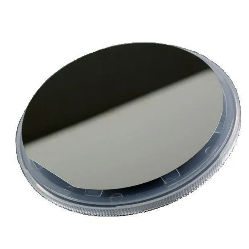
- Sure! Please provide the original title or the news content about Wafer Silicon so I can help rewrite the SEO title without the brand name.
Sure! Please provide the original title or the news content about Wafer Silicon so I can help rewrite the SEO title without the brand name.
By:Admin
Company News & Blog
Rare Earth YAG Crystal Ingot: Everything You Need to Know
YAG Crystal Ingot: A Breakthrough in Semiconductor Material DevelopmentThe semiconductor industry has witnessed a significant breakthrough in the development of YAG Crystal Ingot, a highly advanced material that has the potential to revolutionize the production of high-performance electronic devices. This remarkable achievement is the result of pioneering research and development efforts by a leading semiconductor company, which has successfully synthesized and commercialized the YAG Crystal Ingot for a wide range of applications.The YAG Crystal Ingot, short for Yttrium Aluminum Garnet Crystal Ingot, is a synthetic crystalline material that exhibits exceptional optical and thermal properties. It is widely recognized for its high thermal conductivity, excellent electrical insulation, and superior optical transparency, making it an ideal candidate for a diverse range of semiconductor applications. The unique combination of these properties makes it an attractive material for use in the production of lasers, optical components, and high-performance electronic devices.The successful development of the YAG Crystal Ingot represents a significant milestone in the ongoing pursuit of advanced semiconductor materials. By leveraging the unique properties of the YAG Crystal Ingot, semiconductor manufacturers can enhance the performance, reliability, and efficiency of their products, ultimately driving innovation in various industries including telecommunications, consumer electronics, and automotive technology. With its remarkable attributes, the YAG Crystal Ingot has the potential to enable the development of cutting-edge electronic devices and systems that far surpass the capabilities of current technologies.Behind this groundbreaking achievement is the unwavering commitment and expertise of a leading semiconductor company. This company has dedicated extensive resources to research and development, focusing on the synthesis and commercialization of advanced semiconductor materials. Its team of scientists and engineers have demonstrated a deep understanding of crystal growth, material science, and semiconductor device fabrication, allowing them to successfully produce high-quality YAG Crystal Ingots that meet the stringent requirements of the semiconductor industry.Furthermore, the company has established state-of-the-art manufacturing facilities and quality control processes to ensure the consistency and reliability of its YAG Crystal Ingot products. Through a rigorous and systematic approach to production, the company ensures that each crystal ingot meets the exacting standards of purity, crystalline structure, and optical clarity, meeting the demanding specifications of semiconductor manufacturers.The successful commercialization of the YAG Crystal Ingot has generated significant interest and excitement within the semiconductor industry. Manufacturers and researchers are eager to explore the possibilities and potential applications of this advanced material, recognizing its transformative impact on the development of high-performance electronic devices. With its outstanding thermal and optical properties, the YAG Crystal Ingot is poised to enable the creation of next-generation semiconductor devices, driving new advancements in areas such as high-power laser systems, optical communications, and solid-state lighting.As a result of its remarkable achievements in semiconductor material development, the company has garnered widespread recognition and acclaim within the industry. Its dedication to innovation, research excellence, and product quality has positioned it as a trusted and reliable partner for semiconductor manufacturers seeking advanced materials for their products. With the successful commercialization of the YAG Crystal Ingot, the company has solidified its position as a leader in the advancement of semiconductor materials and technologies.Looking ahead, the remarkable success of the YAG Crystal Ingot is expected to fuel further advancements in semiconductor technology and pave the way for the development of even more advanced materials with enhanced capabilities and performance. As the semiconductor industry continues to push the boundaries of what is possible, the YAG Crystal Ingot stands as a shining example of the potential that groundbreaking research and development can unlock, driving innovation and progress in the field of semiconductor materials and devices.In conclusion, the successful synthesis and commercialization of the YAG Crystal Ingot marks a pivotal moment in the advancement of semiconductor materials and technologies. With its exceptional thermal and optical properties, the YAG Crystal Ingot has the potential to revolutionize the production of high-performance electronic devices, enabling new capabilities and applications across a wide range of industries. As a result of its groundbreaking achievements, the company responsible for the development of the YAG Crystal Ingot has established itself as a leading force in the semiconductor industry, driving innovation and progress with its pioneering research and development efforts.
Laser Ruby Rod: Discover the Latest Advancements in High-Powered Laser Technology
Lasers have revolutionized industries such as medicine, defense, and communication. One crucial component of laser technology is the ruby rod, a cylindrical rod made of synthetic ruby that's lased with flash lamps to produce high-intensity light. A company known for its expertise in producing ruby rods has announced that it has developed a new type of rod that's more efficient, reliable, and durable than traditional models.The company, which has been at the forefront of ruby rod manufacturing for several decades, has announced its latest innovation, called "RubyRod 2.0." According to the company representatives, the new rod is designed to overcome some of the limitations of previous models, such as overheating, crystal cracking, and inconsistent lasing."RubyRod 2.0 is a game-changer for the laser industry," said the company CEO. "Our engineers have worked tirelessly to develop a rod that's not only more efficient and reliable but also more cost-effective than traditional models. We believe that RubyRod 2.0 will set a new standard for ruby rod manufacturing and help our customers to achieve their goals more efficiently and with better results."The new rod is made of advanced materials and features a unique cooling system that prevents overheating, even when lased at high energies for extended periods. It's also designed to minimize crystal cracking, which can lead to loss of efficiency and a shorter lifespan. In addition, RubyRod 2.0 has a consistent lasing output, which ensures that laser systems are stable and reliable.The company has conducted extensive testing and validation of RubyRod 2.0, and the results have been impressive. Independent experts have verified that the new rod outperforms traditional models by a significant margin with respect to energy efficiency, output stability, and durability."We're very excited about RubyRod 2.0," said a spokesperson for a major laser system manufacturer. "We've been using the company's ruby rods for many years, and we've always been impressed with their quality and performance. But RubyRod 2.0 takes it to the next level. We're confident that this new technology will help us to provide better products and services to our customers."The company has also emphasized the environmental benefits of RubyRod 2.0. It's made of non-toxic materials, and its energy-efficient design could help reduce carbon emissions from laser systems, which are often power-hungry.The launch of RubyRod 2.0 is expected to generate significant interest in the laser industry. The company has already received pre-orders from several customers, including major laser system manufacturers, research institutions, and government agencies. The company plans to ramp up production of RubyRod 2.0 to meet the growing demand."We're very optimistic about the future of RubyRod 2.0," said the CEO. "We believe that it will become the go-to choice for companies and organizations that need reliable, efficient, and cost-effective ruby rods. With RubyRod 2.0, we're offering a best-in-class product that's designed to make a positive impact on the laser industry and the world at large." In conclusion, the ruby rod is an essential component of laser technology, and its quality directly affects the performance and reliability of laser systems. The development of RubyRod 2.0 represents a significant leap forward in ruby rod manufacturing, offering better performance, durability, and environmental sustainability to the laser industry. It's an exciting development that will benefit laser system manufacturers, research institutions, and a variety of industries that rely on laser technology.
Discover the Advantages of Gaas Substrate: A Breakthrough in Semiconductor Technology!
[Headline]: Groundbreaking Gaas Substrate Technology Revolutionizes the Semiconductor Industry[Subheadline]: An Introduction to the Company Leading the Transformation[Date][CITY], [STATE] - In an industry that is rapidly advancing and innovating, one company is at the forefront of a major breakthrough that is set to revolutionize the semiconductor industry. By developing and patenting a new Gallium Arsenide (GaAs) substrate technology, this company aims to enhance the performance and efficiency of electronic devices, paving the way for a new era of technological advancements.GaAs substrates have gained significant attention in recent years due to their unique properties and advantages over traditional silicon substrates. This cutting-edge technology enables the creation of devices that are highly efficient, compact, and capable of operating at high frequencies. With an ever-increasing demand for faster, more powerful electronic devices, GaAs substrates have become an attractive alternative to silicon.Leading the charge in GaAs substrate research and development is a pioneering company that has invested significant resources into realizing the full potential of this breakthrough technology. With a team of dedicated scientists, engineers, and researchers, this company has successfully developed a GaAs substrate that surpasses existing industry standards in terms of performance and functionality.One of the key advantages of this GaAs substrate technology relates to its ability to operate at higher frequencies with lower power consumption. This breakthrough ensures that electronic devices utilizing GaAs substrates are not only more energy-efficient but also capable of handling larger data loads. This will have far-reaching implications across a wide range of industries, including telecommunications, aerospace, and consumer electronics.Moreover, this company's GaAs substrate technology offers improved thermal management properties, meaning that devices can operate at higher temperatures without compromising their overall performance. This advancement is particularly crucial in applications such as wireless communication systems and high-speed data transfer, where maintaining signal integrity under extreme conditions is of utmost importance.In addition to these performance enhancements, this GaAs substrate technology also enables smaller device designs. By utilizing the superior conductivity and electron mobility properties of GaAs, electronic components can be made smaller without sacrificing performance. This not only leads to more compact and portable devices but also opens up new possibilities for wearable technology, Internet of Things (IoT) devices, and miniaturized medical devices.Given the immense potential of the GaAs substrate technology developed by this company, they are poised to disrupt the semiconductor industry and drive the next wave of technological advancements. By offering a viable alternative to silicon substrates, this technology ultimately empowers manufacturers to develop electronic devices that are faster, more efficient, and capable of meeting the growing demands of the market.As the global semiconductor industry continues to expand, the commercialization of GaAs substrate technology will undoubtedly play a pivotal role in shaping the future of electronic devices. The innovative efforts and groundbreaking accomplishments of this company represent a significant leap forward in the semiconductor industry, making them a key player in the upcoming era of technological transformation.With ongoing research and development and a commitment to continuous improvement, this company is set to solidify its position as a frontrunner in GaAs substrate technology. As the demand for advanced electronic devices continues to surge, the rapid commercialization of this revolutionary technology is not far off, promising a world where faster, smaller, and more energy-efficient devices reshape our lives.[Concluding paragraph:]In the years to come, the GaAs substrate technology developed by this company will undoubtedly disrupt the semiconductor industry, offering manufacturers and consumers alike a new frontier of possibilities. With its ability to enhance performance, reduce power consumption, and enable smaller device designs, this revolutionary technology is set to reshape the way we interact with electronic devices, catapulting us into a future where innovation knows no boundaries.
Cutting-Edge Wafer Transistor Technology: A Breakthrough in Electronics
Wafer transistor technology is revolutionizing the semiconductor industry with its cutting-edge advancements. With its high-performance characteristics, the technology is increasingly in demand across various sectors such as telecommunications, automotive, and consumer electronics. One company at the forefront of this wave of innovation is {}. With a strong focus on research and development, the company has been a driving force in the development and commercialization of wafer transistor technology. Their commitment to excellence and technological prowess has positioned them as a leader in the industry, and their products are highly sought after by major players in the tech sector.The wafer transistor, a key component in amplifying and switching electronic signals, offers numerous benefits over traditional transistors. With its smaller size, faster speeds, and lower power consumption, it is a game-changer for a wide range of electronic devices. As the demand for smaller and more efficient electronics continues to grow, wafer transistors are becoming increasingly indispensable.The company, {} has been instrumental in pushing the boundaries of wafer transistor technology. Through extensive research and collaboration with leading industry experts, they have been able to develop state-of-the-art wafer transistors that meet the rigorous demands of today's electronic devices. Their commitment to excellence and innovation has made them a trusted partner for companies looking to integrate wafer transistor technology into their products.One of the key drivers of {}’s success is their focus on quality and reliability. Their rigorous testing and quality control processes ensure that their wafer transistors meet the highest standards and deliver exceptional performance. This commitment to excellence has earned them a stellar reputation in the industry and has made them the go-to choice for companies seeking top-notch wafer transistor technology.In addition to their technical prowess, {} is also known for their customer-centric approach. They work closely with their clients to understand their specific needs and provide tailored solutions that meet their requirements. This personalized approach has helped them build strong, long-lasting relationships with their clients and has solidified their position as a trusted partner in the industry.As the demand for wafer transistor technology continues to grow, {} is poised to play a key role in driving its widespread adoption. With their cutting-edge technology, unwavering commitment to quality, and customer-focused approach, they are well-positioned to lead the way in this rapidly evolving field. Their expertise and innovation are set to shape the future of wafer transistor technology and have a profound impact on the electronics industry as a whole.With their track record of excellence and their dedication to pushing the boundaries of wafer transistor technology, {} is set to remain a driving force in the industry for years to come. Their contributions to the advancement of semiconductor technology are invaluable, and their future looks brighter than ever as they continue to innovate and lead the way in wafer transistor technology. As the electronics industry continues to evolve, {} is sure to be at the forefront, shaping the future of wafer transistor technology and driving innovation across the industry.
High Demand for Advanced Semiconductor Wafers in Technology Industry
Inp Wafer is a leading manufacturer of advanced semiconductor products, specializing in the production of high-quality silicon wafers for the global electronics industry. The company is known for its state-of-the-art manufacturing facilities and innovative processes that result in high-performance wafers that are essential for the development of cutting-edge electronic devices. With a commitment to excellence and a focus on continuous improvement, Inp Wafer has earned a reputation as a trusted partner for semiconductor companies around the world.The company's silicon wafers are used in a wide range of electronic applications, including integrated circuits, sensors, and power devices. Inp Wafer's products are known for their exceptional quality and reliability, making them the preferred choice for leading semiconductor manufacturers. The company's dedication to research and development ensures that its wafers meet the demanding requirements of the latest electronic technologies, providing customers with the high-performance materials they need to stay competitive in the global marketplace.Inp Wafer's success is driven by its commitment to customer satisfaction and its ability to consistently deliver top-quality products. The company works closely with its customers to understand their specific needs and develop custom solutions that meet their exact requirements. By providing personalized service and responsive support, Inp Wafer has built strong, long-lasting relationships with its clients and earned their trust and loyalty.As a global leader in the semiconductor industry, Inp Wafer is committed to sustainability and environmental responsibility. The company's manufacturing processes adhere to the highest standards of environmental stewardship, minimizing waste and energy consumption to reduce its carbon footprint. In addition, Inp Wafer actively seeks out opportunities to enhance the recyclability of its products and reduce their impact on the environment. By prioritizing sustainability, the company is not only contributing to a cleaner, healthier planet, but also positioning itself as a responsible and forward-thinking industry leader.Inp Wafer's dedication to excellence, innovation, and sustainability has earned it a leading position in the global semiconductor market. The company's commitment to delivering superior products and outstanding customer service has set it apart as a trusted partner for semiconductor manufacturers worldwide. With a focus on continuous improvement and a passion for exceeding customer expectations, Inp Wafer is poised to continue driving innovation and shaping the future of the electronics industry.
High-quality LiNbO3 Wafer for Advanced Electronic Applications
LiNbO3 Wafer, a key component in the field of integrated optics, has recently made headlines as a revolutionary material that could greatly impact the future of telecommunications and information technology. The wafer, made from lithium niobate, possesses unique optical and electrical properties that make it highly desirable for use in various applications such as modulators, switches, and signal processing devices.The growing demand for LiNbO3 wafers has prompted companies to invest in research and development to meet the needs of the market. One such company is a leading manufacturer of advanced materials and devices for optical communication and high-speed data transmission. With a strong focus on innovation and cutting-edge technology, the company has been at the forefront of developing high-quality LiNbO3 wafers for use in a wide range of applications.The company's LiNbO3 wafers are manufactured using state-of-the-art techniques and adhere to strict quality control processes to ensure the highest level of performance and reliability. These wafers are designed to meet the exacting requirements of customers in the telecommunications industry, where the demand for high-speed data transmission and signal processing is ever-increasing.In addition to their superior optical and electrical properties, LiNbO3 wafers from the company offer excellent mechanical stability and temperature stability, making them ideal for use in harsh operating environments. This level of durability and resilience is a key factor in their widespread adoption in the telecommunications industry, where reliability is paramount.The company's commitment to delivering top-quality LiNbO3 wafers has solidified its position as a trusted partner for customers seeking innovative solutions for their optical communication and data transmission needs. With a strong emphasis on research and development, the company continues to push the boundaries of what is possible with LiNbO3 wafers, constantly seeking new ways to improve performance and efficiency.As the demand for high-speed data transmission continues to grow, the importance of reliable and high-performance components such as LiNbO3 wafers cannot be overstated. With their unique combination of optical, electrical, and mechanical properties, these wafers are poised to play a crucial role in shaping the future of telecommunications and information technology.In conclusion, LiNbO3 wafers are an essential component in the world of integrated optics, with the potential to revolutionize the way information is transmitted and processed. With companies like the one leading the charge in developing high-quality LiNbO3 wafers, the future of telecommunications and information technology looks brighter than ever. As research and development in this field continues to advance, we can expect to see even more groundbreaking innovations that will further improve the performance and reliability of LiNbO3 wafers, paving the way for a more connected and technologically advanced world.
High-Quality and Affordable Laboratory Equipment for Science Experiments
Science Laboratory Equipment, a leading supplier of laboratory equipment and supplies, has been providing high-quality products to scientific institutions, research laboratories, and universities for over a decade. The company offers a wide range of laboratory equipment, including but not limited to, microscopes, centrifuges, spectrophotometers, and analytical balances. Their products are known for their accuracy, reliability, and durability, making them ideal for various scientific applications.In addition to offering a comprehensive selection of laboratory equipment, Science Laboratory Equipment also provides technical support and maintenance services to ensure the proper functioning of their products. Their team of knowledgeable and experienced experts is committed to helping customers find the right equipment for their specific needs and budget.One of the key factors that sets Science Laboratory Equipment apart from other suppliers is their dedication to quality and customer satisfaction. The company sources its products from reputable manufacturers and rigorously tests each item to ensure it meets their high standards. Furthermore, they prioritize customer feedback and continuously strive to improve their product offerings and services.Recently, Science Laboratory Equipment announced the launch of a new line of state-of-the-art laboratory equipment designed to meet the evolving needs of the scientific community. The company's research and development team has been working tirelessly to develop innovative products that will enhance the efficiency and accuracy of scientific experiments.One of the new products introduced by Science Laboratory Equipment is a cutting-edge microscope with advanced imaging capabilities. This microscope is equipped with high-resolution cameras and sophisticated software that allow researchers to capture detailed images and analyze them with precision. The microscope's ergonomic design and user-friendly interface make it easy to use, even for those with limited experience in microscopy.In addition to the microscope, Science Laboratory Equipment has also unveiled a new series of centrifuges that offer unparalleled speed and versatility. These centrifuges feature powerful motors and a range of rotors to accommodate various sample sizes and types. They are designed to deliver fast and efficient separation of substances, making them essential for a wide range of laboratory applications.Furthermore, Science Laboratory Equipment has expanded its range of analytical balances to include models with enhanced accuracy and performance. These balances are equipped with advanced weighing technology and intelligent features that simplify the measurement process and ensure precise results.The launch of these innovative products underscores Science Laboratory Equipment's commitment to staying at the forefront of scientific advancements and meeting the diverse needs of its customers. By investing in research and development, the company aims to empower scientists and researchers with the tools they need to make groundbreaking discoveries and advancements in their respective fields of study.With the introduction of these new products, Science Laboratory Equipment continues to solidify its position as a trusted provider of high-quality laboratory equipment and supplies. The company remains dedicated to helping scientific institutions and researchers achieve their goals by offering cutting-edge solutions and unparalleled support.As Science Laboratory Equipment looks to the future, they are committed to further expanding their product lineup and enhancing their services to better serve the scientific community. Their unwavering dedication to excellence and innovation sets them apart as a leader in the laboratory equipment industry, and they are poised to continue making significant contributions to scientific research and discovery for years to come.
The Advantages of GaN-On-Si Technology for Power Electronics
GaN-On-Si Technology: The Innovative Solution in Power ElectronicsIn recent years, there has been an increasing demand for efficient and reliable power electronics in various industries such as automotive, telecommunications, and renewable energy. As the world continues to move towards a greener and more sustainable future, the need for power electronics that can handle higher power densities while consuming less energy has become essential. This is where GaN-On-Si technology comes into play.GaN-On-Si technology is a groundbreaking innovation that has the potential to revolutionize the power electronics industry. It is a type of semiconductor technology that utilizes gallium nitride (GaN) on a silicon (Si) substrate, offering several advantages over traditional silicon-based power electronics.One company at the forefront of GaN-On-Si technology is {Company X}. They have been leading the way in the development and commercialization of GaN-On-Si technology, offering a wide range of products and solutions for various applications. With their extensive expertise and cutting-edge research and development, {Company X} has positioned themselves as a key player in the power electronics market.{Company X} was founded with the vision of transforming the power electronics industry through innovation and sustainability. Their team of experts has been dedicated to advancing GaN-On-Si technology and bringing it to the mainstream market. With a focus on quality, reliability, and performance, {Company X} has established itself as a trusted partner for businesses looking to integrate GaN-On-Si technology into their products and systems.One of the main advantages of GaN-On-Si technology is its superior performance compared to traditional silicon-based power electronics. GaN-On-Si devices have lower conduction and switching losses, resulting in higher efficiency and reduced power consumption. This makes them ideal for applications that require high power densities and improved energy efficiency, such as electric vehicles, data centers, and renewable energy systems.Another key benefit of GaN-On-Si technology is its ability to operate at higher temperatures and frequencies, making it suitable for harsh and demanding environments. This, combined with its compact size and lightweight nature, makes GaN-On-Si technology a preferred choice for applications where space and weight are critical factors.In addition to performance and reliability, GaN-On-Si technology also offers cost advantages over traditional silicon-based power electronics. The manufacturing process for GaN-On-Si devices is becoming more cost-effective, making them a viable and economical solution for businesses looking to improve their power electronics systems.{Company X} has been instrumental in driving the adoption of GaN-On-Si technology across various industries. They have developed a portfolio of GaN-On-Si devices and solutions that cater to the unique needs of their customers. Whether it's for automotive powertrain systems, high-frequency power supplies, or wireless power transfer, {Company X} has the expertise and resources to deliver high-quality GaN-On-Si products that meet and exceed industry standards.As the demand for efficient and reliable power electronics continues to grow, it is clear that GaN-On-Si technology will play a crucial role in shaping the future of the industry. With {Company X}'s commitment to innovation and sustainability, they are well-positioned to lead the way in advancing GaN-On-Si technology and helping businesses meet their power electronics needs.In conclusion, GaN-On-Si technology represents a significant advancement in the power electronics industry, offering superior performance, reliability, and cost advantages over traditional silicon-based solutions. With {Company X} at the helm of this innovation, businesses can look forward to harnessing the full potential of GaN-On-Si technology and driving the next wave of technological advancements.
Gallium Arsenide: A Revolutionary New Material Taking the Semiconductor Industry by Storm
Galliumarsenide (GaAs) , a compound of gallium and arsenic, has emerged as a crucial material in the development of semiconductors and other electronic devices. The unique properties of GaAs have made it an attractive choice for a wide range of applications, from mobile phone components to solar cells. As the demand for more efficient and powerful electronic devices continues to grow, GaAs has become increasingly important in the technology industry.{} is at the forefront of the use of GaAs in electronic devices. With a strong focus on research and development, {} has been able to harness the unique properties of GaAs to create innovative and high-performance products. The company has a long history of expertise in semiconductor materials, and has proven itself as a leader in the use of GaAs in electronic devices.One of the key advantages of GaAs is its high electron mobility, which allows for the creation of faster and more efficient electronic devices. This has made GaAs an ideal material for high-frequency applications, such as mobile phone components and radio-frequency (RF) devices. In addition, GaAs has a direct bandgap, which allows for the efficient generation and detection of light. This property has made GaAs a popular choice for optoelectronic devices, such as solar cells and light-emitting diodes (LEDs).{} has been able to leverage these properties of GaAs to create a range of cutting-edge electronic devices. The company's GaAs-based products have been widely adopted in the telecommunications industry, where high-frequency and high-speed devices are essential for the transmission of data. In addition, {} has developed a strong presence in the optoelectronics market, with GaAs-based solar cells and LEDs that offer high efficiency and long lifetimes.In recent years, {} has also made significant strides in the development of GaAs-based power devices. These devices are capable of handling high voltages and currents, and are crucial for a range of applications, from power electronics to electric vehicles. {}'s GaAs-based power devices have been well-received in the market, with their high efficiency and reliability making them a preferred choice for a wide range of applications.One of the key strengths of {} is its commitment to research and development. The company has a dedicated team of scientists and engineers who are constantly pushing the boundaries of what is possible with GaAs. By continually exploring new applications and technologies, {} has been able to stay ahead of the curve in the rapidly evolving semiconductor industry.In addition to its technical expertise, {} has also established strong partnerships with leading companies in the semiconductor and electronics industries. This has allowed the company to access the latest technologies and manufacturing processes, ensuring that its GaAs-based products are of the highest quality and performance.Looking to the future, {} is continuing to invest in the development of GaAs-based electronic devices. The company is exploring new applications for GaAs, and is working to further improve the efficiency and performance of its products. With its strong technical expertise and dedication to innovation, {} is well-positioned to remain a leader in the use of GaAs in electronic devices.In conclusion, Galliumarsenide (GaAs) has emerged as a crucial material in the development of high-performance electronic devices. {} has been at the forefront of the use of GaAs in electronic devices, leveraging the unique properties of this material to create innovative and cutting-edge products. With its strong focus on research and development, technical expertise, and commitment to innovation, {} is well-positioned to continue leading the way in the use of GaAs in electronic devices.