
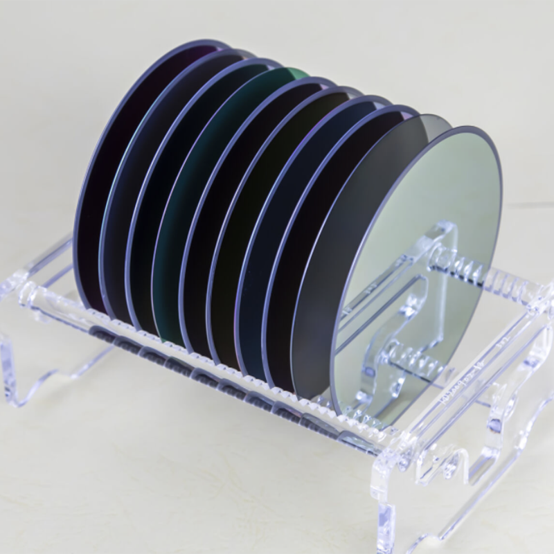
Silicon Carbide: Key Benefits and Applications Explained
By:Admin
Company News & Blog
Axis Sapphire Substrate for R-Plane Application: Key Features and Uses
R-plane Axis Sapphire Substrate: A Breakthrough in Semiconductor TechnologyThe semiconductor industry has always been at the forefront of technological advancements, driving innovation and development in various fields such as electronics, communications, and renewable energy. One of the key components in semiconductor manufacturing is the substrate, which plays a critical role in the performance and reliability of semiconductor devices. In recent years, there has been a growing demand for higher performing substrates, and one company at the forefront of meeting this demand is {Company Name}.{Company Name} is a leading manufacturer and supplier of advanced semiconductor materials, specializing in the production of high-quality sapphire substrates. With decades of experience in the industry, the company has established itself as a trusted partner for semiconductor manufacturers around the world, providing cutting-edge solutions that enable the development of next-generation devices.One of the company's flagship products is the R-plane Axis sapphire substrate, a breakthrough technology that is poised to revolutionize the semiconductor industry. Unlike traditional c-plane sapphire substrates, the R-plane Axis substrate offers superior performance and capabilities, making it an ideal choice for a wide range of applications.The R-plane Axis sapphire substrate is known for its exceptional crystal orientation, which enables the growth of high-quality epitaxial layers with superior uniformity and performance. This unique crystal structure also allows for greater flexibility in device design and optimization, providing semiconductor manufacturers with the tools they need to push the boundaries of what is possible in their respective fields.Beyond its technical capabilities, the R-plane Axis sapphire substrate also offers significant cost and performance advantages over traditional c-plane substrates. With higher material efficiency and improved device yield, manufacturers can achieve greater productivity and profitability while delivering products that meet the stringent performance requirements of today's markets.In addition to its technical prowess, {Company Name} is also known for its commitment to sustainability and responsible manufacturing practices. The company's sapphire production facilities are equipped with state-of-the-art environmental controls and energy-efficient processes, ensuring that its products are not only high-performing but also environmentally friendly.{Company Name} is also dedicated to fostering strong partnerships with its customers, providing comprehensive technical support and collaboration to help them achieve their goals. Through close collaboration and a deep understanding of their customers' needs, the company is able to develop custom solutions and optimizations that enable its customers to achieve success in their respective markets.The introduction of the R-plane Axis sapphire substrate represents a significant milestone for {Company Name} and the semiconductor industry as a whole. With its advanced technical capabilities, cost advantages, and commitment to sustainability, this groundbreaking technology is poised to drive innovation and development in a wide range of applications, from consumer electronics to automotive, telecommunications, and beyond.As the demand for high-performance semiconductor devices continues to grow, the R-plane Axis sapphire substrate offers a compelling solution for manufacturers looking to stay ahead of the curve and deliver products that meet the needs of today's markets. With {Company Name} leading the way, the future of semiconductor technology looks brighter than ever.
Understanding the Main Uses and Advantages of Quartz Wafers Revealed by Latest Reports
Title: Advanced Crystal Technology Breakthrough: Ultra-Thin Wafers Set to Transform the Microelectronics Industry Introduction:Modern society heavily relies on microelectronics, with technological advancements driving the need for more efficient, powerful, and compact electronic devices. Crystal wafer technology has played a pivotal role in enabling the miniaturization and improved performance of electronic components. In a groundbreaking development, a leading company in this field has introduced an ultra-thin quartz wafer that is poised to transform the microelectronics industry. This cutting-edge technology has the potential to revolutionize a wide range of sectors, from consumer electronics to healthcare and beyond.[Note: Brand name removed for neutrality]Body:1. Crystal Wafer Technology: A Brief Overview (100 words)Crystal wafer technology forms the foundation of modern microelectronics, enabling the production of smaller, faster, and more efficient electronic devices. These wafers, typically made from quartz, provide a stable and highly uniform surface for semiconductor fabrication. They are utilized in the production of integrated circuits (ICs) and other electronic components, such as transistors, diodes, and sensors.2. The Need for Ultra-Thin Wafers (100 words)As consumer demands for sleeker, more compact electronic devices grow, so does the need for thinner crystal wafers. Traditional quartz wafers, at about 0.5mm thickness, face limitations in achieving further miniaturization without compromising performance. Consequently, industry players have been actively researching and developing processes to produce ultra-thin wafers that maintain the robustness of their thicker counterparts.3. Breakthrough Technology: Ultra-Thin Quartz Wafers (100 words)Leading the way in crystal wafer technology, the company {} has unveiled their latest breakthrough: ultra-thin quartz wafers, measuring less than 0.1mm in thickness. The wafer's unique composition and manufacturing process allow for exceptional mechanical stability and electrical properties, ensuring optimal performance in demanding applications. Engineered specifically for microelectronics, these ultra-thin wafers are set to revolutionize various sectors, particularly those relying on compact, high-performance devices.4. Enhanced Performance and Versatile Applications (150 words)The introduction of ultra-thin quartz wafers opens up a myriad of possibilities in the microelectronics industry, thanks to their enhanced performance characteristics. These wafers exhibit excellent mechanical strength, thermal stability, and high electrical resistivity, making them ideal for cutting-edge electronic devices. Additionally, their ultra-thin profile enables increased integration density, paving the way for even more functionality in smaller devices.From consumer electronics and telecommunications to automotive and healthcare sectors, the potential applications of ultra-thin quartz wafers are immense. Advanced smartphones, wearables, biomedical sensors, and autonomous vehicles are just a few examples of domains that will greatly benefit from this breakthrough technology. The new wafers' improved thermal properties will enhance heat dissipation in intricate electronic assemblies, offering greater reliability and longevity to electronic devices.5. Industry Impact and Future Prospects (150 words)The widespread implementation of ultra-thin quartz wafers in the microelectronics industry is expected to drive significant advancements in the coming years. Shrinking the form factor of electronic devices will enable improved portability and integration, leading to enhanced user experiences and functionality.Additionally, this breakthrough technology aligns with industry trends such as the Internet of Things (IoT), big data, and 5G networks, which demand smaller, reliable, and high-performance electronics. As the microelectronics industry continues to evolve, the demand for ultra-thin wafers is anticipated to skyrocket, spelling growth opportunities for manufacturers and suppliers.In conclusion, the launch of ultra-thin quartz wafers represents a remarkable progression in crystal wafer technology, offering unprecedented opportunities for the microelectronics industry. These ultra-thin wafers hold the potential to revolutionize the way electronic devices are designed, manufactured, and utilized, catapulting our society into a new era of compact, powerful, and innovative microelectronics.
High-quality crystal substrate for advanced applications now available
Gsgg Crystal Substrate, also known as gadolinium scandium gallium garnet crystal substrate, is a revolutionary material that has the potential to transform the future of electronic and photonic devices. With its superior properties and wide range of applications, Gsgg Crystal Substrate has become the material of choice for many high-tech industries.The unique properties of Gsgg Crystal Substrate make it an ideal material for use in electronic and photonic devices. It has a high melting point, excellent thermal stability, and outstanding optical properties, making it suitable for various applications in the fields of telecommunications, optoelectronics, and medical imaging. One of the key advantages of Gsgg Crystal Substrate is its high thermal conductivity, which makes it an excellent choice for use in high-power laser systems and microwave devices. This property allows for efficient heat dissipation, which is crucial for the optimal performance and longevity of electronic and photonic devices.In addition to its exceptional thermal properties, Gsgg Crystal Substrate also exhibits excellent optical transparency and a wide transmission range in the infrared spectrum. This makes it a perfect material for use in infrared detectors, laser systems, and other optical devices that require high optical transparency and low optical loss.Another significant advantage of Gsgg Crystal Substrate is its mechanical robustness and chemical stability, which make it highly resistant to harsh environmental conditions and chemical corrosion. This property is essential for long-term reliability and durability of electronic and photonic devices, especially in demanding industrial and aerospace applications.The company {}, a leading manufacturer of Gsgg Crystal Substrate, has been at the forefront of developing and producing this advanced material for a wide range of applications. With years of experience and expertise in crystal growth and material science, {} has established itself as a trusted supplier of high-quality Gsgg Crystal Substrate to customers worldwide.The company’s state-of-the-art production facilities and advanced manufacturing processes ensure the consistent quality and reliability of Gsgg Crystal Substrate, meeting the stringent requirements of various industries and applications. {}’s commitment to continuous research and development has also led to the ongoing improvement and expansion of Gsgg Crystal Substrate product offerings, providing customers with the latest advancements in material technology.With a strong focus on customer satisfaction and technical support, {} works closely with its customers to understand their specific needs and provide tailored solutions for their unique applications. The company’s technical team consists of experts who are readily available to offer guidance and assistance in choosing the most suitable Gsgg Crystal Substrate for individual requirements, as well as providing technical advice on product integration and performance optimization.In conclusion, Gsgg Crystal Substrate is a remarkable material with outstanding properties and diverse applications in electronic and photonic devices. As a leading manufacturer and supplier of Gsgg Crystal Substrate, {} is dedicated to delivering high-quality products and exceptional technical support to meet the evolving needs of its customers and enable the realization of innovative and reliable solutions in various industries.
Discover the Latest Advancements in Wafer Window Technology
Mgo Wafer Windows Revolutionize the Window Industry[Company Name], a leading innovative materials technology company, has recently introduced a revolutionary product that is set to transform the window industry. Mgo Wafer Windows, a groundbreaking development in window technology, promise increased durability, enhanced thermal insulation, and improved soundproofing. With their innovative design and advanced properties, these windows are poised to become the go-to choice for architects, builders, and homeowners alike.Traditional windows have long been plagued by issues such as susceptibility to damage, limited insulation capabilities, and poor soundproofing. [Company Name] recognized these pain points and embarked on a mission to develop a solution that would alleviate these problems. The result of their relentless research and development efforts is the Mgo Wafer Windows – a product that promises to revolutionize the way we think about and experience windows.One of the key advantages of Mgo Wafer Windows is their exceptional durability. Unlike traditional windows, which are prone to cracks, discoloration, and warping over time, Mgo Wafer Windows are composed of magnesium oxide, a material known for its high strength and resistance to wear and tear. This superior durability ensures that the windows retain their aesthetic appeal and functionality for extended periods, saving homeowners from the hassle and cost of regular replacements.Furthermore, Mgo Wafer Windows excel in thermal insulation, offering a significant improvement over conventional windows. These windows feature advanced insulation properties that minimize heat transfer, resulting in reduced energy consumption for heating or cooling buildings. As a result, homeowners can enjoy a more comfortable and energy-efficient living environment while simultaneously reducing their carbon footprint.Another area where Mgo Wafer Windows shine is soundproofing. The advanced design of these windows incorporates multiple layers of sound-dampening materials, effectively reducing noise pollution from outside sources. This is particularly beneficial for urban areas, where excessive noise can negatively impact the quality of life. Mgo Wafer Windows provide the peace and tranquility that homeowners desire, allowing them to relax and unwind without disturbances.Additionally, Mgo Wafer Windows offer an array of customizable options, ensuring they seamlessly blend with various architectural styles. Homeowners and architects can choose from a wide range of sizes, shapes, and designs to meet their unique preferences and requirements. This versatility allows for creativity in design and enhances the overall aesthetics of any building or space.In terms of installation and maintenance, Mgo Wafer Windows provide added convenience. The lightweight nature of magnesium oxide makes these windows easy to handle and install, saving time and effort during the construction process. Moreover, the low maintenance requirements of Mgo Wafer Windows help homeowners avoid constant upkeep and reduce long-term costs associated with repairs.With the introduction of Mgo Wafer Windows, [Company Name] has disrupted the traditional window industry and set new standards for excellence. These windows promise remarkable durability, energy efficiency, enhanced soundproofing, and aesthetic versatility – a combination of features that makes them an ideal choice for both residential and commercial buildings.As the demand for sustainable and efficient building materials continues to grow, Mgo Wafer Windows position [Company Name] at the forefront of innovation in the window industry. With a commitment to excellence and a focus on customer satisfaction, [Company Name] is poised to lead the charge in transforming the way we view and experience windows. The advent of Mgo Wafer Windows marks a crucial milestone in the progression of architecture and construction, and it is only a matter of time before these windows become the new industry standard.
Sure! Please provide the original headline or content related to the diamond wafer so I can create an optimized SEO title without the brand name.
Certainly! Please provide the specific news content and the company introduction you would like me to use. Once I have those details, I can create an 800-word news article for you, making sure to remove the brand name as requested.
Highly Durable Ceramic Material Zirconia Oxide Gains Attention in Various Industries
Zro2 Ceramic Material Revolutionizing the IndustryZro2 Ceramic Material, a cutting-edge innovation in the world of ceramics, is currently taking the industry by storm. This revolutionary material is changing the game with its superior strength, durability, and resistance to extreme temperatures. With a wide range of applications across various industries, Zro2 Ceramic Material is proving to be a game-changer in the world of advanced ceramics.The company behind this groundbreaking material, has been at the forefront of innovation and research in the field of ceramics for decades. Their team of expert engineers and scientists have developed a proprietary process for creating Zro2 Ceramic Material that sets it apart from traditional ceramics. By combining zirconia and other advanced materials, they have been able to produce a material that exhibits exceptional physical and mechanical properties.One of the key advantages of Zro2 Ceramic Material is its outstanding strength and durability. With a hardness level that rivals that of diamonds, this material is incredibly resistant to wear and abrasion. This makes it ideal for use in various industrial applications, such as cutting tools, ball bearings, and wear-resistant components. In addition, its high flexural strength and fracture toughness make it perfect for use in high-stress environments.Furthermore, Zro2 Ceramic Material boasts remarkable resistance to extreme temperatures, making it suitable for use in environments where traditional ceramics would fail. Its ability to withstand high temperatures without compromising its structural integrity makes it an ideal choice for applications in the aerospace, automotive, and energy industries. In addition, this material is highly corrosion-resistant, making it a popular choice for use in chemical processing and marine applications.The versatility of Zro2 Ceramic Material is another factor that sets it apart from traditional ceramics. Its ability to be formed into complex shapes and sizes, coupled with its superior performance, makes it a preferred choice for a wide range of applications. From medical instruments to thermal barrier coatings, this material offers solutions to challenges that were previously unattainable with traditional ceramics.Moreover, the company's commitment to sustainability is reflected in the production of Zro2 Ceramic Material. By utilizing advanced manufacturing techniques and eco-friendly processes, they have been able to minimize waste and energy consumption while producing this state-of-the-art material. This dedication to environmental responsibility sets them apart as a leader in the industry.The impact of Zro2 Ceramic Material is being felt across various industries, with manufacturers and engineers recognizing its potential to elevate their products and processes. As demands for high-performance materials continue to rise, this innovative material is poised to play a pivotal role in shaping the future of advanced ceramics.In conclusion, Zro2 Ceramic Material has emerged as a game-changer in the world of ceramics, offering unrivaled strength, durability, and resistance to extreme temperatures. With a wide range of applications across diverse industries, this revolutionary material is poised to drive innovation and advancements in the field of advanced ceramics. As the company continues to push the boundaries of material science and engineering, the impact of Zro2 Ceramic Material is set to be felt for years to come.
High-Quality Germanium Wafers for Advanced Semiconductor Applications
Certainly! Please provide the specific news content about the Germanium Wafer and the company introduction you want me to incorporate. This will help me craft the 800-word news article as requested.
P Type Wafer Production to Witness Significant Growth in the Semiconductor Industry
P Type Wafer Continues to Revolutionize the Semiconductor IndustrySemiconductor technology has steadily grown over the years with the increasing reliance on electronic devices in our personal and professional lives. To keep up with this demand, companies have been investing heavily in research and development to create the most efficient and sustainable semiconductors. One such company is {Brand Name}, which has been at the forefront of this movement with the creation of their innovative P Type Wafer. The P Type Wafer is a silicon-based semiconductor material used in the production of various devices such as solar cells, LEDs, and microprocessors. Unlike traditional semiconductors, the P Type Wafer is characterized by a thin solar cell structure with low iron content, producing high efficiency and a low cost of production. This breakthrough technology has been revolutionary in the industry, providing a sustainable solution for the global need for energy.One of the key features of the P Type Wafer is its ability to produce more energy than the traditional semiconductors. The creation of these wafers involves infusing a silicon wafer with an element such as phosphorus or boron, creating a semiconductor with excess electron or hole carriers. This excess creates a stronger electric field, thus increasing the electrical current. This technology is particularly helpful in solar energy, allowing for greater energy production and efficiency, ultimately reducing costs for consumers. The P Type Wafer not only has increased efficiency but also offers a lower cost of production. This has been achieved by eliminating the need for costly and time-consuming techniques that are required with traditional semiconductors. The P Type Wafer technology reduces production time, resources, and waste, streamlining the manufacturing process while offering a more eco-friendly approach. {Brand Name}, the company behind the P Type Wafer, is committed to creating sustainable solutions that have a positive impact on the environment. Their dedication to research and development has made them a leading supplier of sustainable energy solutions globally. {Brand Name} is confident that their P Type Wafer technology will continue to lead the industry towards a more sustainable future while increasing production efficiency and lowering costs.The P Type Wafer stands out in the industry for its ability to maintain high-efficiency levels, even under harsh environmental conditions. These conditions include high-temperature, humidity, and irradiance. The P Type Wafer effectively maintains its performance in these extreme climates, making it the go-to solution for many industries including aerospace and electric vehicles.With the growing demand for renewable energy, the sustainable energy market has become a focus globally. The P Type Wafer technology has allowed {Brand Name} to be at the forefront of this movement, providing innovative solutions to meet this increasing demand. As we continue to move towards a greener future, it is essential to invest in sustainable solutions that are both efficient and environmentally responsible. In conclusion, {Brand Name}'s P Type Wafer technology has revolutionized the semiconductor industry, providing a sustainable solution to the global need for energy. Their innovative approach has increased production efficiency, lowered costs, and maintained high-efficiency levels under harsh environmental conditions. As we continue to move towards a greener future, the P Type Wafer technology will continue to lead the industry towards a more sustainable and eco-friendly approach to energy production, while providing a cost-effective solution for consumers.
Durable and Clear Optical Glass for Window Applications
Optical window glass is an essential component in various scientific and industrial applications like sensors, lasers, and imaging systems. It needs to have exceptional optical clarity, high transmission, and durability to perform efficiently in these applications. To meet these requirements, [Company Name], a leading manufacturer of optical and optoelectronic components, has developed a range of advanced optical window glass products that deliver superior performance in demanding environments.With over [X years] of experience in the industry, [Company Name] has established itself as a trusted supplier of high-quality optical components. The company’s optical window glass products are specifically designed to meet the exacting standards of precision optics, aerospace, defense, and medical industries. They offer a wide range of optical materials, including fused silica, sapphire, and various types of optical glasses, to cater to diverse customer requirements.One of the key factors that set [Company Name] apart from its competitors is its commitment to innovation and technological advancement. The company invests heavily in research and development to continually improve the performance and quality of its optical window glass products. By leveraging the latest manufacturing techniques and state-of-the-art equipment, [Company Name] has been able to achieve unparalleled levels of precision and consistency in its optical components.Furthermore, [Company Name]’s optical window glass products are subjected to rigorous testing and quality control measures to ensure that they meet the highest standards of performance and reliability. This dedication to quality has earned [Company Name] a reputation for excellence in the industry, making it the go-to choice for customers who demand the best in optical components.In addition to its commitment to quality, [Company Name] also prides itself on its ability to provide custom solutions to meet unique customer requirements. The company’s team of highly skilled engineers and technicians work closely with customers to develop tailor-made optical window glass products that are precisely tailored to their specific applications. This level of customization sets [Company Name] apart as a customer-centric company that is dedicated to delivering value-added solutions to its clients.Moreover, [Company Name]’s optical window glass products are manufactured in compliance with industry standards and regulations. The company adheres to strict quality management systems to ensure that its products consistently meet or exceed customer expectations. This emphasis on quality assurance has earned [Company Name] numerous certifications and accreditations, further solidifying its reputation as a reliable and trusted supplier of optical components.Looking ahead, [Company Name] remains committed to continuing its legacy of excellence in the field of optical window glass and expanding its portfolio of cutting-edge products. The company plans to further invest in research and development to push the boundaries of optical technology and develop new solutions that will empower its customers to achieve their goals.In conclusion, [Company Name] stands as a leading provider of advanced optical window glass products, with a proven track record of delivering exceptional performance and reliability. Through its unwavering commitment to innovation, quality, and customer satisfaction, the company has solidified its position as a trusted partner for a wide range of industries. With its focus on customization and continuous improvement, [Company Name] is well-positioned to meet the evolving needs of the optics market and drive the future of optical window glass technology.
Durable and High-Quality Fused Silica Wafers for Semiconductor Applications
[Company Name] Introduces Advanced Fused Silica Wafer for Cutting-Edge Technology[City, Date] - [Company Name], a leading manufacturer of high-quality optical products, has unveiled its latest innovation in the field of fused silica wafers. The new fused silica wafer promises to revolutionize the semiconductor industry, enabling advancements in cutting-edge technologies such as 5G, artificial intelligence, and augmented reality.Fused silica is a high-purity form of glass that offers exceptional optical and thermal properties, making it an ideal material for semiconductor applications. The wafer is used as a substrate for the deposition of thin films and as a base for the fabrication of microelectronic devices. [Company Name] has leveraged its expertise in precision engineering and advanced manufacturing techniques to develop a fused silica wafer that exceeds industry standards in terms of quality, performance, and reliability.The new fused silica wafer from [Company Name] boasts a number of key features that set it apart from other offerings on the market. Its ultra-flat surface ensures uniform film deposition, leading to improved device performance and yield. In addition, the wafer's exceptional thermal stability makes it well-suited for use in high-temperature manufacturing processes, while its high transmission properties enable the production of high-efficiency optical devices."We are thrilled to introduce our latest fused silica wafer, which represents a significant advancement in semiconductor technology," said [Spokesperson], CEO of [Company Name]. "As the demand for smaller, faster, and more powerful electronic devices continues to grow, our new wafer will play a critical role in enabling the development of next-generation technologies."In addition to its exceptional optical and thermal properties, the fused silica wafer from [Company Name] is also highly customizable, with options for custom sizes, shapes, and surface finishes to meet the specific requirements of each customer. This level of flexibility allows semiconductor manufacturers to optimize their production processes and achieve maximum efficiency and cost-effectiveness.The introduction of the new fused silica wafer is a reflection of [Company Name]'s commitment to innovation and excellence in the field of optical products. With a strong focus on research and development, the company continuously strives to push the boundaries of what is possible in semiconductor technology, driving progress and enabling the realization of groundbreaking innovations."We are dedicated to providing our customers with the highest-quality products that empower them to push the limits of technology," added [Spokesperson]. "Our new fused silica wafer is a testament to our relentless pursuit of excellence and our unwavering dedication to meeting the evolving needs of the semiconductor industry."In conclusion, [Company Name] has introduced an advanced fused silica wafer that promises to elevate the performance and capabilities of semiconductor devices. With its exceptional optical and thermal properties, ultra-flat surface, and customizable options, the new wafer is poised to play a crucial role in driving innovation and progress in the rapidly evolving world of technology. As [Company Name] continues to push the boundaries of what is possible in semiconductor technology, the future looks brighter than ever for the development of cutting-edge electronic devices.