
Durable and High-Quality Fused Silica Wafers for Semiconductor Applications
By:Admin
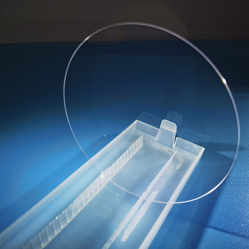
[City, Date] - [Company Name], a leading manufacturer of high-quality optical products, has unveiled its latest innovation in the field of fused silica wafers. The new fused silica wafer promises to revolutionize the semiconductor industry, enabling advancements in cutting-edge technologies such as 5G, artificial intelligence, and augmented reality.
Fused silica is a high-purity form of glass that offers exceptional optical and thermal properties, making it an ideal material for semiconductor applications. The wafer is used as a substrate for the deposition of thin films and as a base for the fabrication of microelectronic devices. [Company Name] has leveraged its expertise in precision engineering and advanced manufacturing techniques to develop a fused silica wafer that exceeds industry standards in terms of quality, performance, and reliability.
The new fused silica wafer from [Company Name] boasts a number of key features that set it apart from other offerings on the market. Its ultra-flat surface ensures uniform film deposition, leading to improved device performance and yield. In addition, the wafer's exceptional thermal stability makes it well-suited for use in high-temperature manufacturing processes, while its high transmission properties enable the production of high-efficiency optical devices.
"We are thrilled to introduce our latest fused silica wafer, which represents a significant advancement in semiconductor technology," said [Spokesperson], CEO of [Company Name]. "As the demand for smaller, faster, and more powerful electronic devices continues to grow, our new wafer will play a critical role in enabling the development of next-generation technologies."
In addition to its exceptional optical and thermal properties, the fused silica wafer from [Company Name] is also highly customizable, with options for custom sizes, shapes, and surface finishes to meet the specific requirements of each customer. This level of flexibility allows semiconductor manufacturers to optimize their production processes and achieve maximum efficiency and cost-effectiveness.
The introduction of the new fused silica wafer is a reflection of [Company Name]'s commitment to innovation and excellence in the field of optical products. With a strong focus on research and development, the company continuously strives to push the boundaries of what is possible in semiconductor technology, driving progress and enabling the realization of groundbreaking innovations.
"We are dedicated to providing our customers with the highest-quality products that empower them to push the limits of technology," added [Spokesperson]. "Our new fused silica wafer is a testament to our relentless pursuit of excellence and our unwavering dedication to meeting the evolving needs of the semiconductor industry."
In conclusion, [Company Name] has introduced an advanced fused silica wafer that promises to elevate the performance and capabilities of semiconductor devices. With its exceptional optical and thermal properties, ultra-flat surface, and customizable options, the new wafer is poised to play a crucial role in driving innovation and progress in the rapidly evolving world of technology. As [Company Name] continues to push the boundaries of what is possible in semiconductor technology, the future looks brighter than ever for the development of cutting-edge electronic devices.
Company News & Blog
Latest News on Semiconductor Wafers: Valuable Insights on Industry Trends and Market Analysis
Title: Silicon Wafer Manufacturer, Inp Wafers, Revolutionizes Semiconductor IndustryIntroduction:Inp Wafers, a leading global manufacturer of high-quality silicon wafers, is reshaping the semiconductor industry with its advanced production techniques and unparalleled product offerings. The company prides itself on delivering cutting-edge solutions to meet the growing demands of the technology sector. Inp Wafers has now unveiled a groundbreaking innovation that promises to further enhance the performance and efficiency of electronic devices. This article explores the recent breakthrough by Inp Wafers, highlighting the potential impact it will have on the semiconductor industry.Body:1. The Importance of Silicon Wafers in Semiconductor Manufacturing:Silicon wafers serve as the foundational material in the production of semiconductors, which are vital components of various electronic devices. These wafers provide the surface where microchips and integrated circuits are built, enabling the creation of smaller, faster, and more powerful electronics. As the demand for high-performing electronic devices continues to surge, manufacturers like Inp Wafers play a crucial role in ensuring the supply of top-quality silicon wafers.2. Inp Wafers Introduces Advanced Manufacturing Technique:In its quest to push the boundaries of semiconductor technology, Inp Wafers has developed an innovative manufacturing technique that promises significant improvements in the efficiency and performance of electronic devices. The company has invested substantial resources in research and development to perfect this groundbreaking method, which combines precision engineering and state-of-the-art materials to create unparalleled silicon wafers.3. Enhanced Performance: The Advantages of Inp Wafers' Innovative Approach:Inp Wafers' advanced manufacturing technique enhances the performance capabilities of silicon wafers, resulting in superior electronic devices. These wafers exhibit remarkably low defect densities, ensuring consistently high yields during the semiconductor fabrication process. Moreover, Inp Wafers' innovative method allows for increased wafer thickness uniformity, enabling manufacturers to achieve precise control over device features. The improved uniformity also enhances transistor performance and reduces power consumption, supporting energy-efficient designs.4. Enhanced Product Offerings: Catering to Diverse Semiconductor Needs:Inp Wafers understands the diverse requirements of its customers and has developed an extensive product range to address specific industry demands. From standard silicon wafers to specialty wafers with unique properties, Inp Wafers offers a comprehensive portfolio to support various semiconductor applications. By providing tailored solutions for different industries, the company ensures that its customers have access to the most appropriate silicon wafers for their specific requirements.5. Partnering for Success: Collaborative Approach:Inp Wafers actively collaborates with leading semiconductor manufacturers, research institutions, and universities to foster innovation and create a vibrant ecosystem. The company recognizes the value of partnerships and invests in collaborative projects to leverage expertise and drive technological advancements. This collaborative approach strengthens the semiconductor industry as a whole, benefiting customers, stakeholders, and end-users alike.6. Sustainable Practices: Inp Wafers' Commitment to the Environment:Inp Wafers is committed to conducting business in an environmentally responsible manner. The company prioritizes sustainable production practices, ensuring minimal waste generation and emissions. With a focus on reducing its carbon footprint, Inp Wafers invests in clean energy alternatives and actively promotes recycling initiatives. By adopting these sustainable practices, the company aligns itself with global efforts to combat climate change and promote a greener future.Conclusion:Inp Wafers, a leading silicon wafer manufacturer, continues to redefine the semiconductor industry through its advanced manufacturing techniques and commitment to innovation. With its groundbreaking approach, Inp Wafers has elevated the performance capabilities of silicon wafers, contributing to the production of faster, smaller, and more energy-efficient electronic devices. As the demand for advanced semiconductors intensifies, Inp Wafers stands at the forefront of providing customized solutions to cater to diverse industry needs. With a collaborative approach and a strong focus on sustainability, Inp Wafers reinforces its commitment to shaping the future of the semiconductor industry.
Durable and Heat-Resistant Quartz Glass: A Breakthrough Material for Various Applications
Quartz glass, also known as fused silica, has long been valued for its exceptional properties and reliability. With its high temperature resistance, excellent thermal shock resistance, and low thermal expansion, quartz glass has become an indispensable material in various industries such as semiconductor manufacturing, optical communication, and laboratory equipment.Quartz glass is made from high-purity silicon dioxide through the process of melting and solidification at extremely high temperatures. This results in a material with a unique combination of mechanical, thermal, and optical properties that make it ideal for a wide range of applications. Its transparency, high chemical purity, and resistance to radiation and high-energy particles have made quartz glass a popular choice for use in high-precision instruments and optical components.As the demand for quartz glass continues to grow, companies like {} have been at the forefront of developing innovative technologies and manufacturing processes to meet the market's needs. {} is a leading manufacturer of quartz glass products, offering a comprehensive range of high-quality quartz glass materials and components for industrial, scientific, and research applications.{}'s quartz glass products are known for their exceptional purity, high precision, and consistent performance. The company's advanced manufacturing facilities and stringent quality control processes ensure that their quartz glass products meet the highest standards and specifications, making them the preferred choice for customers around the world.One of the key attributes of {}'s quartz glass products is their high resistance to thermal shock and rapid temperature changes. This makes them especially suitable for use in high-temperature applications such as furnace tubes, wafer carriers, and semiconductor processing equipment. Their superior thermal stability and low coefficient of thermal expansion also make {}'s quartz glass products an excellent choice for optical lens elements, photomask substrates, and other precision optical components.In addition to their thermal properties, {}'s quartz glass products also exhibit excellent electrical insulation and high transmission of ultraviolet, visible, and infrared light. These characteristics make them highly valuable for use in ultraviolet lamps, wafer inspection systems, and spectroscopy instruments, where high optical clarity and minimal light absorption are essential.{}'s commitment to continuous improvement and innovation has led to the development of new quartz glass formulations and production techniques that further enhance the performance and versatility of their products. By leveraging their expertise in material science and engineering, {} is able to tailor their quartz glass products to meet the specific requirements of their customers, ensuring optimal performance and reliability in their applications.With a strong focus on research and development, {} is constantly exploring new applications and markets for their quartz glass products. By collaborating with customers and industry partners, {} is able to identify emerging trends and technologies, and develop tailored solutions that address the evolving needs of the market.As the demand for high-performance materials continues to grow in industries such as semiconductor manufacturing, optical communication, and photovoltaics, companies like {} play a crucial role in providing the essential building blocks that enable technological advancements and innovation. Through their dedication to excellence and customer satisfaction, {} is well-positioned to continue leading the way in the development and production of high-quality quartz glass products for a wide range of applications.
Sic Wafer Market Trends and Growth Analysis
Sic Wafer, a key player in the semiconductor industry, recently announced a major breakthrough in the development of silicon carbide (SiC) wafers. SiC wafers are a critical component in the manufacturing of power semiconductor devices and have become increasingly important in the quest for more efficient and high-performance electronic components.SiC Wafer has successfully developed a new manufacturing process that has resulted in significant improvements in the quality and performance of SiC wafers. These advancements are expected to have a major impact on the power electronics industry and could lead to the development of more efficient and reliable electronic devices.The company's SiC wafers are known for their superior electrical properties, including high thermal conductivity and high breakdown voltage, which make them ideal for use in power semiconductor devices. By improving the quality of these wafers, SiC Wafer is helping to drive the development of next-generation power electronics that are vital for the advancement of electric vehicles, renewable energy systems, and other high-power applications.Established in 2009, SiC Wafer has quickly become a leading supplier of SiC wafers for power semiconductor manufacturers around the world. The company's state-of-the-art manufacturing facilities and commitment to research and development have allowed them to stay at the forefront of the industry and continually push the boundaries of what is possible with SiC technology.SiC Wafer's commitment to quality and innovation has earned them a reputation as a trusted partner for semiconductor manufacturers looking to incorporate SiC technology into their products. Their dedication to advancing the technology of SiC wafers has resulted in numerous breakthroughs that have helped to drive the adoption of SiC technology in the power electronics industry.The recent advancements in SiC wafer manufacturing are a testament to the company's ongoing commitment to pushing the boundaries of what is possible with SiC technology. By continually improving the quality and performance of SiC wafers, SiC Wafer is helping to drive the development of more efficient and reliable electronic devices that are essential for the transition to a more sustainable and electrified future.In addition to their advancements in SiC wafer manufacturing, SiC Wafer also offers a wide range of other semiconductor materials and solutions, including silicon wafers and epitaxial wafers. Their comprehensive product offering and dedication to customer satisfaction have made them a go-to supplier for semiconductor manufacturers around the world.With a strong track record of innovation and a commitment to providing the highest quality semiconductor materials, SiC Wafer is well-positioned to continue leading the way in the development of SiC technology. Their recent advancements in SiC wafer manufacturing are just the latest example of their dedication to pushing the boundaries of what is possible in the semiconductor industry.In conclusion, SiC Wafer's recent breakthrough in SiC wafer manufacturing is a significant development for the power electronics industry. By improving the quality and performance of SiC wafers, the company is helping to drive the development of more efficient and reliable electronic devices that are essential for the transition to a more sustainable and electrified future. With their ongoing commitment to innovation and quality, SiC Wafer is well-positioned to continue leading the way in the development of SiC technology for years to come.
Durable and High-Quality Fused Silica Wafers for Semiconductor Applications
[Company Name] Introduces Advanced Fused Silica Wafer for Cutting-Edge Technology[City, Date] - [Company Name], a leading manufacturer of high-quality optical products, has unveiled its latest innovation in the field of fused silica wafers. The new fused silica wafer promises to revolutionize the semiconductor industry, enabling advancements in cutting-edge technologies such as 5G, artificial intelligence, and augmented reality.Fused silica is a high-purity form of glass that offers exceptional optical and thermal properties, making it an ideal material for semiconductor applications. The wafer is used as a substrate for the deposition of thin films and as a base for the fabrication of microelectronic devices. [Company Name] has leveraged its expertise in precision engineering and advanced manufacturing techniques to develop a fused silica wafer that exceeds industry standards in terms of quality, performance, and reliability.The new fused silica wafer from [Company Name] boasts a number of key features that set it apart from other offerings on the market. Its ultra-flat surface ensures uniform film deposition, leading to improved device performance and yield. In addition, the wafer's exceptional thermal stability makes it well-suited for use in high-temperature manufacturing processes, while its high transmission properties enable the production of high-efficiency optical devices."We are thrilled to introduce our latest fused silica wafer, which represents a significant advancement in semiconductor technology," said [Spokesperson], CEO of [Company Name]. "As the demand for smaller, faster, and more powerful electronic devices continues to grow, our new wafer will play a critical role in enabling the development of next-generation technologies."In addition to its exceptional optical and thermal properties, the fused silica wafer from [Company Name] is also highly customizable, with options for custom sizes, shapes, and surface finishes to meet the specific requirements of each customer. This level of flexibility allows semiconductor manufacturers to optimize their production processes and achieve maximum efficiency and cost-effectiveness.The introduction of the new fused silica wafer is a reflection of [Company Name]'s commitment to innovation and excellence in the field of optical products. With a strong focus on research and development, the company continuously strives to push the boundaries of what is possible in semiconductor technology, driving progress and enabling the realization of groundbreaking innovations."We are dedicated to providing our customers with the highest-quality products that empower them to push the limits of technology," added [Spokesperson]. "Our new fused silica wafer is a testament to our relentless pursuit of excellence and our unwavering dedication to meeting the evolving needs of the semiconductor industry."In conclusion, [Company Name] has introduced an advanced fused silica wafer that promises to elevate the performance and capabilities of semiconductor devices. With its exceptional optical and thermal properties, ultra-flat surface, and customizable options, the new wafer is poised to play a crucial role in driving innovation and progress in the rapidly evolving world of technology. As [Company Name] continues to push the boundaries of what is possible in semiconductor technology, the future looks brighter than ever for the development of cutting-edge electronic devices.
A Guide to Different Types of Glasses Lens Materials
Glasses Lens Type Revolutionizes the Eyewear IndustryIn today's fast-paced world, technology and innovation are constantly driving change and progress in various industries. The eyewear industry is no exception, as breakthroughs in lens technology continue to improve the quality of vision for individuals with vision issues. One company that has been at the forefront of this advancement is {}.{} is a leading manufacturer and supplier of eyewear lenses, with a strong focus on innovation and quality. The company has been dedicated to providing cutting-edge solutions to improve the vision of individuals around the world. With a team of experienced professionals and state-of-the-art facilities, {} has been able to develop and produce some of the most advanced lenses in the industry.One of the latest breakthroughs to come out of {} is the development of a new glasses lens type that is set to revolutionize the eyewear industry. This new lens type has been designed to provide exceptional clarity and comfort for individuals with a wide range of vision issues. Whether it's nearsightedness, farsightedness, or astigmatism, these new lenses are able to provide a high level of correction and visual acuity.One of the key features of these new lenses is their advanced material composition, which allows for a thinner and lighter lens compared to traditional options. This not only enhances comfort for the wearer but also provides a more aesthetically pleasing look for the glasses. In addition, the lenses are also equipped with advanced coatings that reduce glare, improve scratch resistance, and provide UV protection, ensuring long-term durability and performance.Another significant aspect of these new lenses is their versatility. {} has designed them to be compatible with a wide range of frames, allowing individuals to choose from various styles and designs to suit their personal preferences. This level of customization and adaptability is a game-changer for the eyewear industry, as it provides customers with more options and flexibility when it comes to finding the perfect pair of glasses.Furthermore, {} has also ensured that these new lenses are easily accessible to individuals around the world. By working with a network of optometrists, ophthalmologists, and eyewear retailers, the company has made it possible for customers to have access to these innovative lenses. This ensures that individuals can receive professional guidance and fitting services to ensure that the new lenses meet their specific vision needs.The impact of these new glasses lenses from {} is expected to be significant in the eyewear industry. With their advanced technology, improved comfort, and enhanced visual clarity, they are set to raise the bar for what customers can expect from their eyewear. As a result, {} is positioned to continue leading the way in innovation and setting new standards for the industry as a whole.In conclusion, the development of this new glasses lens type by {} is a testament to the company's commitment to pushing the boundaries of innovation in the eyewear industry. By combining advanced technology, exceptional quality, and a dedication to customer satisfaction, {} has created a product that is set to revolutionize the way individuals experience and interact with their vision correction. As a result, the future looks bright for both {} and the customers who will benefit from these groundbreaking lenses.
How to Increase the Speed of Your Computer with this Simple Hack
Microsoft, in partnership with leading technology company Apple, has made an exciting announcement about the release of the latest version of its operating system, Windows. The new version, Windows 11, is set to revolutionize the way we use our devices and promises to provide a seamless and innovative user experience.Windows 11 is the result of Microsoft's ongoing commitment to innovation and technological advancement. The operating system is designed to be more intuitive and user-friendly, with a focus on productivity and creativity. With a sleek and modern interface, Windows 11 aims to deliver a seamless and efficient experience for both personal and professional users.In addition to the improved user interface, Windows 11 also introduces a range of new features and capabilities. One of the most notable additions is the integration of a virtual assistant, which will provide users with personalized support and assistance. This virtual assistant is designed to help users navigate the operating system and perform tasks more efficiently, making it easier to access important information and complete everyday tasks.Furthermore, Windows 11 also offers enhanced security features to protect users' data and privacy. The operating system includes built-in security tools and features, such as advanced encryption and secure browsing, to help users stay safe online and protect their sensitive information from cyber threats.The collaboration between Microsoft and Apple has played a significant role in the development of Windows 11. By combining Microsoft's expertise in software development with Apple's innovative hardware technologies, the two companies have created an operating system that is tailored to the needs of modern users. The result is a powerful and versatile operating system that combines the best of both worlds, offering a seamless and intuitive user experience across a wide range of devices.With the release of Windows 11, Microsoft is also introducing a range of new products and services to complement the operating system. These include new hardware devices, such as laptops and tablets, that are designed to take full advantage of the capabilities of Windows 11. In addition, Microsoft is also launching a range of software applications and services that are optimized for use with Windows 11, providing users with a comprehensive and seamless ecosystem of products and services.In summary, Windows 11 represents a significant step forward in the evolution of operating systems. With its innovative features, intuitive interface, and seamless user experience, Windows 11 is set to revolutionize the way we use our devices and is poised to become the operating system of choice for both personal and professional users. The collaboration between Microsoft and Apple has played a crucial role in the development of Windows 11, and the result is a powerful and versatile operating system that is tailored to the needs of modern users. With the release of Windows 11, Microsoft is also introducing a range of new products and services that are designed to complement the operating system, creating a comprehensive ecosystem of products and services for users to enjoy.
Discover the Beauty and Versatility of Glass Block
Title: Innovative Glass Block Enhances Structural Integrity and Architectural Aesthetics for Sustainable Building Design[City, Date] - (Company Name), a global leader in architectural solutions, has unveiled their latest product, an innovative Glass Block that combines cutting-edge technology with unparalleled functionality. This state-of-the-art solution offers architects and construction professionals the perfect balance of structural integrity and artistic appeal, revolutionizing sustainable building design.Designed to meet the ever-evolving needs of the modern construction industry, the (Glass Block) by (Company Name) aims to create visually stunning and energy-efficient spaces while ensuring durability and reliability. With its ingeniously engineered design, this glass block provides an ideal solution for architects, interior designers, and contractors seeking to create sustainable, aesthetically pleasing structures.What sets the (Glass Block) apart is its exceptional strength and versatility. This product is constructed using the highest quality materials to ensure a robust and long-lasting structure, making it suitable for use in both commercial and residential projects. Employing advanced manufacturing techniques, the (Glass Block) offers enhanced resistance to breakage, impacts, and adverse weather conditions while maintaining its transparency and visual appeal.Moreover, this glass block's distinct design features make it an excellent choice for improving energy efficiency within buildings. The advanced insulation capabilities of the (Glass Block) significantly contribute to reducing heating and cooling costs by minimizing heat transfer. This not only enhances the overall comfort level of the space but also promotes sustainability by reducing the building's carbon footprint.The (Glass Block) is available in a wide range of sizes, shapes, and finishes, allowing architects and designers to unleash their creativity and realize their unique visions. Whether it's creating an open-plan office space that maximizes natural light or incorporating an eye-catching feature wall in a residential setting, this glass block offers endless design possibilities.Furthermore, (Company Name) prides itself on delivering high-quality products that align with eco-friendly principles. The (Glass Block) is no exception, as it is designed to meet and exceed industry standards for sustainability. Committed to reducing environmental impact, the company employs sustainable manufacturing practices, ensuring minimal waste generation and maximizing resource efficiency.The development of this groundbreaking glass block is a testament to (Company Name)'s continued commitment to innovation and customer satisfaction. By combining exceptional functionality with exquisite aesthetics, the (Glass Block) has the potential to reshape the way architects and designers approach sustainable building design.As one of the industry leaders, (Company Name) has made significant contributions to architectural advancements. With a wide range of successfully completed projects globally, the company has gained a reputation for delivering excellence and pushing the boundaries of what is possible in the industry.The newly introduced (Glass Block) is set to revolutionize architectural design by providing an attractive and structurally sound material that contributes to more sustainable buildings. With its enhanced strength, energy efficiency, and aesthetic appeal, the (Glass Block) by (Company Name) is poised to become a popular choice among architects, builders, and interior designers alike.In conclusion, (Company Name)'s latest offering, the (Glass Block), showcases their unwavering commitment to innovation, sustainability, and excellence in architectural solutions. With its remarkable strength and design versatility, this glass block offers architects and designers the opportunity to create truly extraordinary structures that merge aesthetic perfection and environmental consciousness.
Breakthrough in Semiconductor Technology: A Revolutionary New C Plane for Sapphire Crystal
Introducing the Revolutionary Sapphire C Plane: Transforming the Future of AviationIn a groundbreaking development for the aviation industry, a leading aerospace company has unveiled the state-of-the-art Sapphire C Plane. With its cutting-edge technology and innovative design, the Sapphire C Plane is set to revolutionize the way we fly, offering unparalleled efficiency, sustainability, and passenger comfort. This game-changing aircraft is the latest addition to the company's impressive portfolio, solidifying their position as pioneers in aviation advancement.The Sapphire C Plane, meticulously engineered by a team of experts, boasts a unique configuration that optimizes performance, making it one of the most efficient and eco-friendly aircraft in its class. Its advanced aerodynamics, revolutionary lightweight materials, and state-of-the-art propulsion system all contribute to its impressive fuel efficiency, reducing emissions and minimizing its carbon footprint. In an era where reducing environmental impact is paramount, the Sapphire C Plane sets a new standard for sustainable aviation.Passenger comfort and experience have also been given significant attention in the design process of the Sapphire C Plane. The innovative cabin layout prioritizes passenger well-being, offering a spacious and luxurious environment. The aircraft's interior includes meticulously designed seating arrangements, which optimize legroom and personal space, ensuring a comfortable journey for all passengers. The cutting-edge entertainment system provides state-of-the-art technology for in-flight entertainment, offering an immersive experience throughout the flight.Not only does the Sapphire C Plane prioritize passenger comfort, but it also ensures their safety through its industry-leading safety features. Extensive research and development have gone into creating an aircraft that exceeds standard safety regulations. The integration of advanced collision avoidance systems, enhanced turbulence dampening technologies, and highly intelligent autopilot systems ensures a safe and secure journey for all passengers on board.In addition to being environmentally friendly and comfortable, the Sapphire C Plane also offers unparalleled speed and efficiency. Its cutting-edge propulsion system provides exceptional thrust, allowing for faster travel times and more efficient operations. This increase in efficiency translates to cost savings for airlines, which can have a positive impact on ticket prices for passengers. With its incredible speed and efficiency, the Sapphire C Plane enables connectivity and accessibility to a wider array of destinations.The company behind this revolutionary aircraft has a long-standing reputation for innovation and excellence in the aerospace industry. With a rich history of pioneering groundbreaking technologies, they continue to push the boundaries of what is possible in aviation. The introduction of the Sapphire C Plane reaffirms their commitment to advancing the field, revolutionizing the future of flight.Looking ahead, the Sapphire C Plane represents a significant milestone in aviation history, paving the way for a new era of sustainable, efficient, and safe air travel. As the industry adapts to meet the growing demand for eco-friendly and passenger-oriented solutions, the Sapphire C Plane sets a new standard for excellence. With its advanced technologies and unrivaled performance, this aircraft is primed to shape the future of air transportation, providing a seamless journey for passengers while minimizing environmental impact.
Advancements in Monocrystalline Silicon Wafers: A Breakthrough in Semiconductor Technology
[Assistant]Title: Paving the Way for Advanced Solar Technology: Monocrystalline Silicon WaferIntroduction (40 words):Innovating the future of renewable energy, Monocrystalline Silicon Wafers, produced by a leading solar technology company, are revolutionizing solar power generation. This cutting-edge technology harnesses sunlight with unrivaled efficiency, positioning it as a breakthrough solution in the renewable energy sector.Body:I. Background on Monocrystalline Silicon Wafer (220 words)Monocrystalline Silicon Wafers are the foundation of high-performance solar panels. Made from a single crystal structure, their unique design allows them to absorb sunlight more effectively than other types of solar cells. This efficiency translates into increased energy output and a more sustainable approach to power generation.Monocrystalline Silicon Wafers offer several key advantages, including exceptional durability, high conversion efficiency, and advanced aesthetics. These properties make them the preferred choice for manufacturers and consumers alike, driving the growth of the global solar energy market. By utilizing this technology, we can significantly reduce our reliance on fossil fuels and mitigate the deleterious effects of climate change.II. Company Introduction: (250 words){Company Name}, a renowned pioneer in the field of solar technology, has been at the forefront of developing and optimizing Monocrystalline Silicon Wafer manufacturing processes. Established in {year}, the company has consistently delivered cutting-edge solutions and contributed to the rapid advancement of solar energy use worldwide.{Company Name}'s commitment to research and development has enabled them to create Monocrystalline Silicon Wafers that offer the highest conversion efficiency levels currently available. This efficient energy conversion leads to an increased power output, allowing end-users to maximize their solar investment while minimizing their carbon footprint.Moreover, {Company Name} has dedicated significant resources to enhance the durability and reliability of their Monocrystalline Silicon Wafers. Through innovations in material science and manufacturing techniques, they ensure that their products withstand harsh weather conditions and maintain their performance over an extended period.Additionally, {Company Name} places great emphasis on the aesthetics of their solar panels. Understanding the importance of blending renewable energy solutions seamlessly into architectural designs, they offer Monocrystalline Silicon Wafers with a sleek and uniform appearance. This commitment to visual integration opens up new possibilities for incorporating solar power generation into various landscapes and urban environments.III. Market Impact and Future Prospects (290 words)The widespread adoption of Monocrystalline Silicon Wafers has significantly boosted the solar energy market. With their superior efficiency and performance, these wafers are rapidly becoming the industry standard for solar panel manufacturers. As a result, global solar energy installations have experienced exponential growth, contributing to a substantial reduction in greenhouse gas emissions.The increasing demand for renewable energy solutions, coupled with technological advancements, has led to a considerable decrease in production costs. This cost reduction has made solar energy more accessible to a broader consumer base, further driving the adoption of Monocrystalline Silicon Wafers.Looking ahead, {Company Name} continues to invest in research and development to enhance the efficiency and versatility of their Monocrystalline Silicon Wafers. Their goal is to improve energy conversion rates, reduce manufacturing costs, and explore new applications for this groundbreaking technology.In conclusion, Monocrystalline Silicon Wafers, pioneered by {Company Name}, offer a game-changing solution for the renewable energy sector. Their superior efficiency, durability, and aesthetics position them as the cutting-edge choice for solar power generation. As the technology and market for Monocrystalline Silicon Wafers continue to evolve rapidly, we can anticipate a brighter and more sustainable future powered by the sun.
High-quality Sapphire Wafer for A-Plane Axis Applications
A-plane Axis, a cutting-edge technology company, recently announced the launch of their revolutionary sapphire wafer for use in the aerospace industry. This breakthrough product promises to revolutionize the way planes are designed and built, by providing a more durable and reliable material for use in critical components.The A-plane Axis sapphire wafer is made from high-purity synthetic sapphire, a material known for its exceptional hardness and resistance to wear and corrosion. This makes it ideal for use in aerospace applications, where components are subjected to extreme conditions and must withstand high levels of stress and wear.The unique properties of sapphire make it an excellent choice for use in critical components such as bearings, seals, and other parts that are subjected to high levels of friction and wear. Its exceptional hardness and wear resistance make it far superior to traditional materials such as metal alloys or ceramics, which are more prone to wear and degradation over time.In addition to its exceptional durability, the A-plane Axis sapphire wafer also offers other key advantages for aerospace applications. Its high thermal conductivity and excellent electrical insulation properties make it well-suited for use in high-temperature and high-voltage applications, where traditional materials may struggle to perform.Furthermore, the use of sapphire in aerospace components can also lead to significant weight savings, as it is a lightweight material compared to traditional metal alloys. This can contribute to overall fuel efficiency and reduce the environmental impact of aircraft operations, a key consideration for the aviation industry.The launch of the A-plane Axis sapphire wafer represents a major milestone for the company, which has positioned itself as a leader in advanced materials technology for aerospace applications. With a strong focus on research and development, A-plane Axis has invested heavily in the development of new and innovative materials to meet the evolving needs of the aerospace industry.The company's state-of-the-art manufacturing facilities and cutting-edge production techniques enable them to produce sapphire wafers with exceptional precision and consistency, ensuring that they meet the stringent quality standards required for aerospace applications.A-plane Axis's sapphire wafer is already gaining attention from leading aerospace manufacturers, who are keen to take advantage of its unique properties to improve the performance and reliability of their aircraft. With the potential to enhance the durability, efficiency, and safety of aerospace components, the use of sapphire wafers could have a transformative impact on the industry as a whole.In addition to aerospace applications, A-plane Axis is also exploring the potential use of sapphire wafers in other industries, such as semiconductor manufacturing, automotive, and medical devices. The versatility and unique properties of sapphire make it a promising material for a wide range of applications, and the company is committed to exploring new opportunities for its use.As the aerospace industry continues to evolve and demand for more advanced materials grows, A-plane Axis is well-positioned to be at the forefront of this technological revolution. With its innovative sapphire wafer, the company is poised to make a lasting impact on the way aircraft are designed and built, leading to safer, more efficient, and more reliable air travel for years to come.