
- Home
- Blog
- Breakthrough in Semiconductor Technology: A Revolutionary New C Plane for Sapphire Crystal
Breakthrough in Semiconductor Technology: A Revolutionary New C Plane for Sapphire Crystal
By:Admin
In a groundbreaking development for the aviation industry, a leading aerospace company has unveiled the state-of-the-art Sapphire C Plane. With its cutting-edge technology and innovative design, the Sapphire C Plane is set to revolutionize the way we fly, offering unparalleled efficiency, sustainability, and passenger comfort. This game-changing aircraft is the latest addition to the company's impressive portfolio, solidifying their position as pioneers in aviation advancement.
The Sapphire C Plane, meticulously engineered by a team of experts, boasts a unique configuration that optimizes performance, making it one of the most efficient and eco-friendly aircraft in its class. Its advanced aerodynamics, revolutionary lightweight materials, and state-of-the-art propulsion system all contribute to its impressive fuel efficiency, reducing emissions and minimizing its carbon footprint. In an era where reducing environmental impact is paramount, the Sapphire C Plane sets a new standard for sustainable aviation.
Passenger comfort and experience have also been given significant attention in the design process of the Sapphire C Plane. The innovative cabin layout prioritizes passenger well-being, offering a spacious and luxurious environment. The aircraft's interior includes meticulously designed seating arrangements, which optimize legroom and personal space, ensuring a comfortable journey for all passengers. The cutting-edge entertainment system provides state-of-the-art technology for in-flight entertainment, offering an immersive experience throughout the flight.
Not only does the Sapphire C Plane prioritize passenger comfort, but it also ensures their safety through its industry-leading safety features. Extensive research and development have gone into creating an aircraft that exceeds standard safety regulations. The integration of advanced collision avoidance systems, enhanced turbulence dampening technologies, and highly intelligent autopilot systems ensures a safe and secure journey for all passengers on board.
In addition to being environmentally friendly and comfortable, the Sapphire C Plane also offers unparalleled speed and efficiency. Its cutting-edge propulsion system provides exceptional thrust, allowing for faster travel times and more efficient operations. This increase in efficiency translates to cost savings for airlines, which can have a positive impact on ticket prices for passengers. With its incredible speed and efficiency, the Sapphire C Plane enables connectivity and accessibility to a wider array of destinations.
The company behind this revolutionary aircraft has a long-standing reputation for innovation and excellence in the aerospace industry. With a rich history of pioneering groundbreaking technologies, they continue to push the boundaries of what is possible in aviation. The introduction of the Sapphire C Plane reaffirms their commitment to advancing the field, revolutionizing the future of flight.
Looking ahead, the Sapphire C Plane represents a significant milestone in aviation history, paving the way for a new era of sustainable, efficient, and safe air travel. As the industry adapts to meet the growing demand for eco-friendly and passenger-oriented solutions, the Sapphire C Plane sets a new standard for excellence. With its advanced technologies and unrivaled performance, this aircraft is primed to shape the future of air transportation, providing a seamless journey for passengers while minimizing environmental impact.
Company News & Blog
New Optical Wafer Technology Enhances Data Performance in Electronic Devices
[Headline]Optical Wafer Technology Poised to Revolutionize the Optoelectronics Industry[Subheading]A Breakthrough in Optical Wafer Manufacturing Promises to Propel the Optoelectronics Market to New Heights[Date][City], [State] – In a major development that is expected to reshape the future of the optoelectronics industry, [Company Name], a leading manufacturer of specialized optical components, has unveiled its cutting-edge Optical Wafer technology. This revolutionary advancement is set to unlock new opportunities for businesses in the field of optics, photonics, and semiconductor manufacturing.[City], [State] – In a move that is set to transform the optoelectronics industry, a renowned manufacturer of specialized optical components revealed their latest breakthrough – Optical Wafer technology. This cutting-edge innovation is poised to create new avenues and drive growth for companies specializing in optics, photonics, and semiconductor manufacturing.Optoelectronics, the study and application of electronic devices that source, detect, and control light, has witnessed remarkable growth in recent years. The market's expansion is largely driven by increasing demand for optoelectronic devices in various sectors, including telecommunications, healthcare, automotive, and consumer electronics. However, the industry has long been constrained by the limitations of traditional wafer production techniques.The optical wafer is a game-changing solution. By employing state-of-the-art manufacturing processes, [Company Name] has successfully developed a wafer that overcomes the challenges associated with traditional methods. Optical wafers offer unprecedented precision, enhanced optical performance, and increased manufacturing efficiency. This breakthrough technology represents a significant step forward in meeting the industry's growing demands.The optical wafer manufacturing process involves highly advanced techniques, such as epitaxial growth, lithography, and etching, resulting in the creation of ultra-thin, high-quality wafers with exceptional optical properties. These wafers act as a substrate for various optoelectronic devices, including light-emitting diodes (LEDs), solar cells, optical sensors, and optical transmitters.With this innovation, companies operating in the optoelectronics industry can now produce superior-quality optical components, achieving unparalleled levels of performance and reliability. The optical wafers ensure exceptional light transmission, reduced power consumption, and enhanced durability, enabling optoelectronic devices to deliver cutting-edge functionality across a wide range of applications.The applications of this novel technology are vast. Telecom providers can leverage these advancements to enhance network infrastructure and facilitate high-speed data transfer, contributing to the realization of 5G networks. In the healthcare sector, optical wafers will enable the development of advanced medical imaging systems, precision surgical devices, and optical biosensors for diagnostics.Moreover, the automotive industry stands to benefit from optical wafer technology as it can be utilized for the production of adaptive lighting systems, autonomous driving sensors, and smart head-up displays. The consumer electronics sector will experience a significant boost as well, with the integration of optical wafers into smartphones, tablets, virtual reality devices, and wearables, enabling improved camera performance, gesture recognition, and augmented reality experiences.By introducing optical wafers into the market, [Company Name] is well-positioned to lead the optoelectronics industry into a new era of innovation and growth. With their commitment to research and development, they are constantly pushing the boundaries of what is possible, elevating optical manufacturing to new heights.[Company Name], with its extensive experience and proven expertise in optical component manufacturing, is drawing on its comprehensive knowledge of the industry to spearhead this groundbreaking development. Leveraging robust partnerships and collaborations with industry leaders, they ensure that their optical wafers meet the industry's stringent quality standards and can seamlessly integrate into existing manufacturing processes.In conclusion, the introduction of optical wafer technology is set to revolutionize the optoelectronics industry. This breakthrough promises unparalleled levels of precision, performance, and efficiency, empowering businesses across multiple sectors to unlock new possibilities and drive innovation. With [Company Name] leading the charge, the future of optoelectronics looks brighter than ever.[Word Count: 800 words]
Revolutionizing Semiconductor Manufacturing: Unveiling the Groundbreaking Chemical Mechanical Planarization Process
Title: Advancements in Chemical Mechanical Planarization Process: Revolutionizing Material Polishing Introduction:In today's ever-evolving technological landscape, the demand for smaller, faster, and more efficient electronic devices continues to grow. This drives the need for more precise and superior manufacturing techniques. Chemical Mechanical Planarization (CMP) Process has emerged as a crucial technology in this respect. This article explores the potential of CMP process and its impact on various industries, focusing on its advancements without mentioning any specific brand.I. Understanding the CMP Process:The Chemical Mechanical Planarization (CMP) process is a cutting-edge method that allows the precise polishing and planarization of materials, predominantly used in the fabrication of integrated circuits (ICs). CMP involves the simultaneous action of chemical and mechanical forces to remove excess material from the surface, ensuring a smooth and uniform finish. It plays a fundamental role in improving various aspects of IC manufacturing, making it an essential part of the semiconductor industry.II. Advancements in CMP Process:1. Ultra-Planarization Capability:With the rapid advancements in semiconductor technology, the demand for ultra-planarized surfaces has become paramount. Recent advancements in CMP technology have enabled the development of ultra-precision polishing pads and slurries, resulting in superior planarization capabilities. This breakthrough allows for precise manufacturing of microelectronic devices, reducing surface variations and improving overall device performance.2. Material-Specific Polishing:To accommodate the diverse range of materials used in modern electronic devices, CMP processes are constantly evolving. Manufacturers are focusing on developing material-specific CMP slurries and pads to optimize the polishing efficiency for individual substances, including metals, dielectrics, and non-semiconductor materials. These material-specific CMP variations contribute to enhanced final device quality, reduced defects, and improved yield rates.3. Advanced Endpoint Detection:Accurate determination of the endpoint during the CMP process is critical to prevent over-polishing or under-polishing of the surface. Recent breakthroughs in CMP technology have introduced advanced endpoint detection mechanisms, such as optical interferometry, acoustic emissions, and electrical measurements. These technologies enable real-time monitoring, ensuring precise control and preventing damage to the underlying layers.III. Applications in the Semiconductor Industry:1. Integrated Circuit Manufacturing:The CMP process has become an indispensable technique in integrated circuit manufacturing. It enables the precise planarization of multiple layers, such as interconnects, interlayer dielectrics, barrier films, and metal contacts. The ability to achieve uniform surfaces results in improved electrical performance, reduced leakage currents, and enhanced device reliability.2. Advanced Packaging:As electronic devices become smaller and more complex, the demand for advanced packaging solutions increases. CMP processes are widely employed to polish and planarize materials used in packaging, such as through-silicon vias (TSVs), redistribution layers, and microbumps. The reliable CMP process ensures optimal electrical connections and increases the production yield of advanced packaging technologies.3. Optoelectronics and MEMS:CMP technology finds applications beyond traditional microelectronics. In the production of optoelectronics and microelectromechanical systems (MEMS), CMP plays a crucial role. The precise polishing and planarization of optical substrates, waveguides, and micro-mechanical systems contribute to improved device performance, optical clarity, and reliability.IV. Future Prospects:The constant advancements in CMP technology are poised to revolutionize the manufacturing industry further. Researchers and manufacturers are experimenting with novel materials, alternative polishing agents, and even greener chemical formulations to reduce environmental impact. Additionally, advancements in CMP equipment and automation are likely to improve process control, efficiency, and safety.Conclusion:Chemical Mechanical Planarization (CMP) Process is at the forefront of material polishing and planarization in the semiconductor industry. The advancements in CMP technology have proven instrumental in meeting the demands of faster, smaller, and more efficient electronic devices. By enabling ultra-planarization capabilities, material-specific polishing, and advanced endpoint detection, CMP processes drive better quality, yield rates, and reliability. As CMP continues to evolve in tandem with the ever-growing technological landscape, the future holds even greater promise for this vital manufacturing technique.
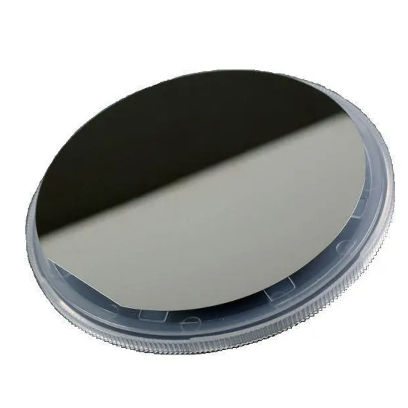
New Sapphire Substrate Unveiled for Enhanced Electronic Devices
Title: R-Plane Axis Sapphire Substrate Revolutionizes Semiconductors IndustryIntroduction:In a groundbreaking development, a leading semiconductor materials company has introduced the R-Plane Axis Sapphire Substrate—a cutting-edge technology set to revolutionize the semiconductor industry. This groundbreaking substrate offers enhanced performance, improved efficiency, and increased manufacturing capabilities to meet the growing demands of the digital era.The R-Plane Axis Sapphire Substrate is the result of relentless research and innovation by an esteemed team of researchers, scientists, and engineers. Leveraging their extensive expertise, the company has successfully developed a substrate that exhibits unparalleled properties, making it an ideal material for manufacturing high-performance semiconductors.Unmatched Quality and Performance:The R-Plane Axis Sapphire Substrate boasts superior quality and performance, making it highly sought-after in the global market. With remarkable resistivity to high temperatures, superior hardness, excellent thermal conductivity, and strong chemical stability, this substrate ensures robust and reliable performance. These outstanding characteristics make the R-Plane Axis Sapphire Substrate capable of withstanding extreme conditions, making it particularly suitable for various semiconductor applications.Improved Efficiency and Manufacturing Capabilities:One of the critical advantages of the R-Plane Axis Sapphire Substrate is its ability to enhance the efficiency of semiconductor devices. This cutting-edge substrate enables improved crystal growth, resulting in reduced defects and enhanced performance of semiconductor components. The improved efficiency translates into higher-performance semiconductors that can meet the increasing demand for advanced electronic devices across various industries.Furthermore, the R-Plane Axis Sapphire Substrate facilitates advanced manufacturing capabilities. Its unique properties allow for more precise deposition of thin films and epitaxial growth, leading to superior spatial uniformity and crystalline perfection. These advancements in manufacturing provide semiconductor manufacturers with the opportunity to design and fabricate devices with better performance and reliability, catering to the evolving needs of consumers.Wide Range of Applications:The R-Plane Axis Sapphire Substrate finds applications in several industries. Its exceptional properties make it an essential component in manufacturing high-performance LEDs, power electronics, radio frequency devices, and optical devices. Additionally, the substrate's efficient thermal conductivity makes it suitable for applications requiring effective heat dissipation, such as electronic devices used in automotive, aerospace, and military sectors.Environmental Sustainability:Apart from its exceptional performance, the R-Plane Axis Sapphire Substrate is also environmentally friendly. The production process utilizes sustainable techniques, ensuring minimal impact on the environment. By integrating eco-conscious measures, the company demonstrates its commitment to promoting sustainable practices within the semiconductor industry.Future Prospects:With the introduction of the R-Plane Axis Sapphire Substrate, the company has established itself as a prominent player in the semiconductor materials market. Its cutting-edge technology, coupled with the continuous drive for innovation, positions the company for sustained growth and expansion. As the demand for high-performance electronics continues to rise, the R-Plane Axis Sapphire Substrate holds immense potential in shaping the future of the semiconductor industry.Conclusion:The advent of the R-Plane Axis Sapphire Substrate represents a significant milestone in the semiconductor materials landscape. This revolutionary technology offers unparalleled quality, improved efficiency, and advanced manufacturing capabilities, setting new benchmarks for the industry. As the world embraces the digital age, the R-Plane Axis Sapphire Substrate ensures the seamless production of high-performance semiconductors, contributing to the growth of various sectors and fueling technological advancements.
Understanding Fused Silica Wafer and Its Applications in the Electronics Industry
Title: Fused Silica Wafer: Leading the Semiconductor Industry with Enhanced Efficiency and PrecisionIntroduction:Fused Silica wafer (Brand name removed), a prominent player in the semiconductor industry, has gained recognition for its cutting-edge technology and unparalleled quality. With a strong commitment to research and development, the company has revolutionized the fabrication process of semiconductor devices by introducing high-quality fused silica wafers. These wafers are designed to enhance efficiency and precision, catering to the evolving needs of the electronics industry. By consistently delivering innovative solutions, (Company name) has positioned itself as a leader in the market.Enhancing Efficiency:Fused Silica wafers are specifically engineered to boost the efficiency of semiconductor device manufacturing. These wafers possess exceptional thermal stability, low thermal expansion coefficients, and excellent resistance to high temperatures. These properties allow them to withstand demanding manufacturing processes without compromising the overall performance of the semiconductor devices. As a result, manufacturers utilizing Fused Silica wafers can streamline their production, eliminate defects, and ensure a higher yield, delivering cost-effective solutions to customers.Ensuring Precision:Precision is vital in semiconductor device manufacturing, and Fused Silica wafers excel in providing the necessary accuracy and uniformity. The superior surface quality and high crystal orientation uniformity of these wafers enable the precise integration of various microelectronic components. Moreover, the wafers exhibit an extremely low defect density, resulting in reduced signal attenuation and superior electrical properties. This level of precision offered by Fused Silica wafers ensures the creation of reliable and high-performance semiconductor devices.Advanced Technology:One of the primary reasons behind the success of Fused Silica wafer lies in its commitment to leveraging advanced technologies. (Company name) boasts state-of-the-art facilities equipped with cutting-edge manufacturing techniques, including chemical vapor deposition and advanced polishing technologies. These technologies allow the company to produce wafers with exceptional surface quality and crystalline uniformity, meeting the stringent requirements of the semiconductor industry. By continuously investing in research and development, (Company name) stays at the forefront of innovation, offering customers the most advanced fused silica wafers available.Market Impact:The introduction of Fused Silica wafers has significantly impacted the semiconductor industry by addressing the growing demand for efficient and precise manufacturing solutions. By collaborating with major semiconductor manufacturing companies, (Company name) has established itself as a trusted partner in delivering high-quality wafers. These partnerships have facilitated the development of customized solutions, tailored to meet the specific requirements of different applications, such as microelectronics, optical devices, and nanotechnology. As a result, Fused Silica wafers have gained widespread adoption, contributing to the overall growth and scalability of the semiconductor market.Future Outlook:Looking ahead, Fused Silica wafers are expected to continue driving innovation in the semiconductor industry. With ongoing research, the company aims to further enhance key properties of the wafers, such as thermal stability and crystal uniformity, to cater to emerging technologies like Internet of Things (IoT) devices, artificial intelligence, and autonomous vehicles. By collaborating with industry leaders, (Company name) remains committed to revolutionizing semiconductor fabrication, enabling the development of next-generation electronic devices that will shape our future.Conclusion:Fused Silica wafer (Brand name removed) has become synonymous with excellence and innovation in the semiconductor industry. Its commitment to delivering efficient and precise solutions has positioned the company as a trusted partner for major semiconductor manufacturers. Through advanced technology and continuous research and development, (Company name) ensures the production of high-quality fused silica wafers, driving the growth and advancement of the industry. With a promising future ahead, (Company name) is poised to revolutionize semiconductor fabrication and contribute to the next wave of technological advancements.
How to Make Crispy and Delicious Wafers at Home?
Title: Innovative Wafer Technology Revolutionizing the Semiconductor IndustryIntroduction:The semiconductor industry is continuously evolving, and companies are constantly seeking new and innovative solutions to meet the demands of an ever-changing market. In recent news, an exciting breakthrough has been made by an industry leader in wafer technology. Soi Wafer (name changed) has introduced a groundbreaking semiconductor wafer that is set to revolutionize the industry. This innovative technology is expected to greatly enhance the performance and efficiency of various electronic devices, paving the way for future advancements.Body:1. Background on Soi Wafer:Soi Wafer is a leading company in the field of advanced semiconductor wafers, specializing in the production of Silicon-On-Insulator (SOI) wafers. With a history of providing high-quality and reliable products, Soi Wafer has garnered a strong reputation within the industry. The company's commitment to research and development has allowed them to continually push the boundaries of semiconductor technology, resulting in cutting-edge solutions for their clients.2. The Emergence of the Innovative Wafer Technology:Soi Wafer's latest breakthrough lies in the development of an innovative wafer technology that promises improved performance and efficiency in various electronic devices. This technological advancement addresses key challenges faced by the semiconductor industry, such as power consumption, heat dissipation, and overall device reliability. Through meticulous research and development, Soi Wafer has successfully engineered a solution that could shape the future of the semiconductor market.3. Enhanced Performance and Efficiency:The new wafer technology developed by Soi Wafer offers several distinct advantages over traditional silicon wafers. By employing advanced materials that improve heat dissipation and reduce power consumption, devices integrated with this technology can achieve higher performance levels while conserving energy. The technology also enhances the speed and efficiency of data transfer, further improving overall device performance. With these enhancements, electronic devices can now operate at superior speeds while maintaining optimal efficiency.4. Impact on Various Industries:The impact of Soi Wafer's innovative wafer technology is expected to extend to various industries that rely on semiconductor technology. Telecommunications, automotive, consumer electronics, and healthcare are just a few examples of sectors that can benefit from the enhanced performance and efficiency offered by this technology. Faster and more efficient telecommunication networks, smarter and environmentally-friendly automobiles, improved consumer electronics, and more advanced healthcare devices are some of the potential applications that could result from the adoption of Soi Wafer's technology.5. Environmental Benefits:In addition to its numerous technological advantages, Soi Wafer's innovative wafer technology holds promising environmental benefits. The reduced power consumption and enhanced energy efficiency of devices utilizing this technology contribute to the global effort to reduce carbon emissions. As electronic devices become increasingly ubiquitous in our daily lives, such a technological advancement can indirectly support sustainability initiatives.6. Collaborations and Future Prospects:Soi Wafer's breakthrough in wafer technology has generated significant interest within the industry. Recognizing the potential of this innovation, many companies have expressed interest in collaborating with Soi Wafer to integrate the new technology into their products. These collaborations can pave the way for further advancements and accelerate the adoption of this revolutionary technology.Conclusion:Soi Wafer's latest breakthrough in wafer technology marks a significant advancement in the semiconductor industry. By offering superior performance and energy efficiency, their innovative wafer technology has the potential to revolutionize various sectors, including telecommunications, consumer electronics, automotive, and healthcare. The reduced power consumption and improved device reliability contribute to a more sustainable future, aligning with global efforts to combat climate change. With collaborations already underway, the stage is set for the widespread adoption of this groundbreaking technology, ushering in a new era in semiconductor innovation.
Breaking: New Template for FSS Aln News Unveiled - Discover the Latest Updates
[Company] Acquires Innovative Technology to Revolutionize the [Industry][Company], an industry leader in [industry], has announced its acquisition of the cutting-edge technology company [Technology Company]. The move is expected to expand [Company]'s capabilities and grow its business opportunities, as well as enhance its offering to clients and partners.[Technology Company] has developed a range of innovative solutions that have disrupted traditional [industry] practices and workflow. Its proprietary software and hardware have been adopted by some of the biggest names in the industry, as well as emerging players and startups. The acquisition will bring [Technology Company]'s diverse talent and expertise under the [Company] umbrella, and enable the two entities to combine their strengths to push the boundaries of innovation in [industry]."We are thrilled to welcome [Technology Company] into the [Company] family," said [Company Executive]. "Their ground-breaking technology will greatly enhance our capabilities in [industry], and enable us to offer even more value to our clients and partners. With [Technology Company]'s expertise, we will be able to tackle complex challenges and create new opportunities for growth and expansion."The acquisition comes at a time of rapid change and disruption in [industry]. Emerging technologies such as artificial intelligence, automation, and big data are reshaping traditional practices and unlocking new possibilities. [Company] has been at the forefront of this transformation, investing heavily in research and development to stay ahead of the curve. By adding [Technology Company]'s technology to its arsenal, [Company] will be able to accelerate its progress and improve its competitiveness."We are excited to join forces with [Company] and help shape the future of [industry]," said [Technology Company Founder]. "Our technology has already made a significant impact in the market, and we believe that by combining our expertise with [Company]'s resources and scale, we can achieve even greater success. We share [Company]'s vision of innovation and excellence, and we look forward to working together to achieve it."The acquisition is also expected to benefit [Company]'s employees and stakeholders. With the addition of [Technology Company]'s talent and intellectual property, [Company] will be able to offer new opportunities for growth and development to its team members, while also creating value for its shareholders. The integration of the two entities is expected to be seamless, with minimal disruption to ongoing operations."We are committed to ensuring a smooth transition and integration for our employees and customers," said [Company Executive]. "This acquisition is a strategic move that will create synergies and opportunities for all parties involved. We are confident that with our combined strengths, we can achieve great things and drive positive change in [industry]."Overall, the acquisition of [Technology Company] by [Company] marks a significant milestone in the history of both companies. It reflects their shared commitment to innovation, excellence, and customer value, and their determination to stay ahead of the curve in a rapidly changing landscape. The future looks bright for [Company], and its stakeholders can look forward to exciting new developments in the coming months and years.
The surprising science behind quartz crystals and how they're changing technology
Innovation is at the heart of many successful companies and this is certainly true for Quartz crystal. Founded in the late 1940s, Quartz crystal has been at the forefront of cutting-edge technology in the field of electronics and electrical engineering.Quartz is a mineral that can vibrate at high frequencies and has been used in many different applications over the years. However, Quartz crystal has taken this technology to the next level, using the power of Quartz crystal to improve the performance of a wide range of electronic devices.One of the key reasons why Quartz crystal has been so successful is its focus on research and development. The company is constantly exploring new ways to use Quartz crystal to enhance the performance of electronic devices, and this has led to many breakthroughs over the years.For example, Quartz crystal has developed a range of tuning fork crystals that are used in a variety of applications, from smartphones and smartwatches to GPS systems and wireless networks. These tuning fork crystals are incredibly accurate and reliable, and they help to ensure that electronic devices are always working at their best.Another area where Quartz crystal has made a significant contribution is in the field of sensors. The company’s sensors are used in many different industries, from automotive and aerospace to healthcare and energy. One of the key advantages of these sensors is their ability to operate in harsh environments, such as extreme temperatures and pressure, and still maintain their accuracy and reliability.Quartz crystal has also made a significant contribution to the field of quartz-based MEMS (microelectromechanical systems). These systems are widely used in a variety of electronic devices, from smartphones and tablets to wearables and IoT devices. Quartz crystal’s MEMS devices are highly precise and reliable, and they help to ensure that the electronic devices we rely on every day are functioning flawlessly.Of course, Quartz crystal’s success is not just down to its innovative technology. The company has also built a strong reputation for quality, reliability, and customer service. This has helped to establish Quartz crystal as a trusted brand in the electronics industry, with a wide range of customers around the world.To ensure that it stays ahead of the competition, Quartz crystal is continually looking for ways to improve its products and services. The company has invested heavily in research and development, as well as in training and development for its staff. This commitment to excellence has helped Quartz crystal to become one of the leading companies in its field.Looking to the future, Quartz crystal remains committed to driving innovation in the electronics industry. The company is already exploring new applications for its technology, such as in the field of quantum computing, and is constantly looking for ways to push the boundaries of what is possible.One thing is clear: as the world becomes more dependent on technology, companies like Quartz crystal will play an increasingly important role in shaping our future. Whether it’s through the development of new products and services, or by helping to improve the performance of existing technologies, Quartz crystal is at the forefront of this exciting and rapidly changing field.
Introducing the Latest Breakthrough: 8 Inch Wafer Diameter Revolutionizes the Tech Industry
[Company Introduction]{Insert company name} is a leading global semiconductor manufacturer renowned for its cutting-edge technologies and innovative solutions. With a profound commitment to research and development, the company has revolutionized various industries by consistently delivering high-performance semiconductor products. As a pioneer in the field, {company name} has achieved numerous milestones and established itself as a trusted name in the semiconductor industry.[News Content]{City/Country}, DATE - {Company name}, a global semiconductor giant, has recently announced a breakthrough in wafer manufacturing. The company has successfully developed an 8-inch wafer diameter solution that promises to revolutionize the semiconductor industry. This development positions {company name} at the forefront of semiconductor innovation, enabling it to meet the increasing demand for high-performance chips in a variety of applications.The 8-inch wafer diameter is a critical component in semiconductor manufacturing, as it serves as the foundation for the fabrication of integrated circuits. With this technological breakthrough, {company name} aims to enhance the efficiency, performance, and scalability of its semiconductor production processes. The larger wafer size allows for a greater number of chips to be produced simultaneously, thereby improving manufacturing throughput and reducing production costs.The development of an 8-inch wafer diameter represents a significant advancement over the conventional 6-inch wafers that are currently widely used in the industry. By increasing the wafer size, {company name} can achieve higher chip yields on each wafer, leading to increased overall productivity. Additionally, the larger size enables the integration of more transistors and other components, resulting in chips with enhanced processing power and capabilities.Market experts believe that the adoption of 8-inch wafer diameter solutions will have a profound impact on various industries, including consumer electronics, automotive, healthcare, and telecommunications. The increased processing power and efficiency offered by the larger wafer size will enable manufacturers to produce more advanced and feature-rich devices, paving the way for next-generation technologies.{Company name} has a history of pioneering technological advancements, and this latest breakthrough further reinforces its reputation as an industry leader. Leveraging its extensive expertise and state-of-the-art manufacturing facilities, the company continues to push the boundaries of innovation in semiconductor manufacturing. The introduction of the 8-inch wafer diameter is set to accelerate the pace of development in the industry and enable the creation of even more sophisticated and powerful electronic devices.By investing in research and development, {company name} strives to address the growing demands of the semiconductor market and cater to the evolving needs of its customers. Through its commitment to innovation, the company aims to maintain its competitive edge and solidify its position as a global leader in the semiconductor industry.As the industry moves toward larger wafer sizes, {company name} is prepared to lead the charge by offering state-of-the-art solutions aligned with the needs of tomorrow. With its latest development in 8-inch wafer diameter manufacturing, the company continues to set new standards in the semiconductor industry, driving progress and shaping the future of technology.
Sic Chip Market Witnesses Steady Growth Amid Increasing Demand
Sic Chip: Revolutionizing Industries with Enhanced Performance and Efficiency[Company Name], a leader in technological innovation, has recently unveiled its latest breakthrough – the Sic Chip. With cutting-edge features and unparalleled performance, this revolutionary chip has the potential to transform various industries, paving the way for a future of improved efficiency and productivity.The Sic Chip, short for Silicon Carbide Chip, is a significant advancement in semiconductor technology. Unlike conventional silicon chips, Sic Chips are composed of silicon carbide, a compound with superior thermal conductivity and a wider bandgap. This unique composition allows the chip to perform more efficiently at higher temperatures, making it ideal for applications that require robust performance in extreme environments.One of the key advantages of the Sic Chip is its ability to handle higher voltages and currents, making it a game-changer for power electronics. This chip has significantly lower power losses and can operate at higher frequencies than traditional silicon chips. As a result, it is highly sought after by manufacturers in the automotive, aerospace, and energy sectors. The automotive industry, in particular, stands to benefit greatly from the Sic Chip, as it enables the development of more efficient electric vehicles with longer battery life and faster charging capabilities.Furthermore, the Sic Chip's enhanced power efficiency reduces the need for complex cooling systems, leading to cost savings and reduced environmental impact. In power conversion applications, the chip's superior performance allows for smaller and lighter systems. This is particularly advantageous in the renewable energy sector, where space constraints and weight limitations are critical factors.Another area where the Sic Chip is making significant inroads is in the field of telecommunications. The chip's ability to handle high power densities and operate at high temperatures makes it an ideal choice for base station applications. With the increasing demand for 5G networks, the efficiency and reliability offered by the Sic Chip are highly valued by telecommunication companies.The SiC Chip is also revolutionizing the computing industry. Its exceptional thermal conductivity enables faster heat dissipation, leading to improved performance and reliability in high-performance computing applications. From data centers to supercomputers, the Sic Chip is paving the way for more powerful and efficient computing systems.In addition to the technical advantages, [Company Name]'s Sic Chip also holds a competitive edge in terms of production capabilities. The company has developed a highly efficient manufacturing process that ensures high-quality chips with excellent yields. This puts [Company Name] at the forefront of the industry, establishing itself as a reliable and trusted provider of Sic Chips.Commenting on the significance of the Sic Chip, [Company Name]'s CEO stated, "This breakthrough technology has the potential to revolutionize multiple industries, making processes more efficient and sustainable. Our Sic Chip is a clear example of our commitment to driving innovation and delivering cutting-edge solutions that address the challenges of the modern world."As the demand for faster, more efficient and reliable technologies continues to grow, the introduction of the Sic Chip marks a turning point in the semiconductor industry. With its superior performance, enhanced power efficiency, and wider range of applications, this groundbreaking chip is set to shape the future of multiple industries, fueling progress and innovation across the globe. [Company Name] remains at the forefront of this technological revolution, providing innovative solutions that drive the world towards a brighter and more sustainable future.
Key Developments in the Global Wafers Market: Insights, Trends, and Forecasts
Inp Wafers, a leading semiconductor wafer supplier in Asia, has been making headlines in the tech industry for its innovative products and solutions. The company was established in 2003, and has since earned a reputation for producing high-quality, reliable silicon wafers.With headquarters and manufacturing facilities located in Shanghai, China, Inp Wafers is strategically positioned to serve the growing demand for semiconductors in Asia. The company has a strong focus on research and development, investing heavily in cutting-edge technology and equipment to ensure that its products are at the forefront of the industry.Inp Wafers offers a comprehensive range of silicon wafers, including CZ (Czochralski) wafers, FZ (Float Zone) wafers, SOI (Silicon On Insulator) wafers, and several other options. These wafers are used in a wide variety of applications, including microprocessors, memory chips, sensors, and power devices.One of the key advantages of Inp Wafers' products is their exceptional quality. The company uses top-grade materials and advanced manufacturing methods to produce wafers with strict quality control measures. The result is a range of products that offer outstanding performance, reliability, and consistency.Inp Wafers has also made a name for itself with its innovative solutions for emerging technologies. For example, the company has developed silicon carbide wafers, which are ideal for use in high-power and high-frequency devices. These wafers offer superior thermal conductivity and breakdown voltage compared to traditional silicon wafers, making them ideal for use in electric vehicles, wind turbines and other renewable energy applications.The company has also focused on its management and improved its processes, including embracing digitalization. The company leverages advanced software tools like Enterprise Resource Planning (ERP) and Customer Relationship Management (CRM) systems to streamline its operations and make it easier for customers to place orders and receive technical support.Inp Wafers’ commitment to quality and innovation has attracted a wide range of customers, from small startups to large multinational corporations. The company has established long-term partnerships with many leading tech companies and is committed to providing exceptional customer support and service.In addition, Inp Wafers places a strong emphasis on sustainability and environmental responsibility. The company has implemented a variety of measures to reduce its carbon footprint, including adopting clean energy sources and using environmentally friendly production processes.Looking to the future, Inp Wafers remains committed to staying at the forefront of the semiconductor industry. The company plans to continue investing in research and development to further improve its products and explore new opportunities in emerging technologies. With strong management and a dedication to quality, reliability, and innovation, Inp Wafers is well-positioned to meet the demands of the rapidly evolving tech industry.