
High-Quality LiNbO3 Ingot for Advanced Applications
By:Admin
Company News & Blog
High-quality Fused Silica Substrate for Various Applications
Fused Silica Substrate: The Foundation of Cutting-Edge TechnologyFused silica substrate, also known as fused quartz, is a key component in the manufacturing of advanced optical and electronic systems. Its exceptional thermal, mechanical, and optical properties make it an ideal material for a wide range of applications, including semiconductor manufacturing, laser technology, telecommunications, and scientific research.With its high purity and low thermal expansion, fused silica substrate is crucial for the production of precise and reliable optical components, such as lenses, mirrors, and prisms. Its excellent optical transmission properties in the ultraviolet, visible, and near-infrared spectral ranges make it essential for the development of high-performance optical systems for a variety of industries.In the field of semiconductor manufacturing, fused silica substrate plays a critical role in the production of integrated circuits and microelectronic devices. Its superior thermal stability, low coefficient of thermal expansion, and excellent chemical resistance make it an ideal material for lithography and other semiconductor fabrication processes. Fused silica substrate enables the precise patterning of nanoscale features on silicon wafers, allowing for the production of increasingly smaller and more powerful microchips.Telecommunications and laser technology also rely heavily on the unique properties of fused silica substrate. Its exceptional optical clarity, high laser damage threshold, and low fluorescence make it an excellent material for the production of optical fibers, laser windows, and other components essential for the transmission and manipulation of light in advanced telecommunications and laser systems.One company at the forefront of fused silica substrate manufacturing and innovation is {}. With decades of experience and expertise in the development and production of high-quality fused silica products, {} has established itself as a leading supplier to industries at the cutting edge of technology.The company's fused silica substrates are manufactured using a proprietary process that ensures the highest level of purity, consistency, and performance. Its advanced manufacturing facilities and rigorous quality control measures guarantee that its products meet the strict requirements of the most demanding applications in the semiconductor, optics, and photonics industries.{} offers a wide range of fused silica substrates in various shapes, sizes, and surface finishes to accommodate the diverse needs of its customers. Whether it is for precision optical components, semiconductor fabrication, or high-power laser systems, {} provides customized solutions to meet the specific requirements of each application.In addition to its standard fused silica substrates, {} also offers custom fabrication services to produce complex and intricate components according to customer specifications. Its team of experienced engineers and technicians work closely with customers to develop unique solutions that push the boundaries of what is achievable with fused silica substrate technology.Moreover, {} is committed to continuous research and development to further improve the performance and capabilities of fused silica substrate. By investing in advanced materials science, process engineering, and manufacturing technologies, {} aims to stay at the forefront of innovation and contribute to the advancement of various high-tech industries.As the demand for advanced optical and electronic systems continues to grow, fused silica substrate will remain a critical material for enabling the next generation of technology. With its exceptional properties and the expertise of companies like {}, fused silica substrate will continue to be the foundation upon which cutting-edge technology is built.
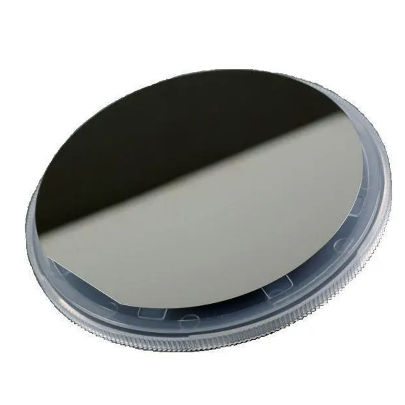
Latest Test Wafers Unveiled: A Major Breakthrough Shaping the Semiconductor Industry
**Title: Test Wafers: Revolutionizing Semiconductor Testing Industry with Cutting-Edge Technology**Introduction:In the rapidly advancing semiconductor industry, efficient and accurate testing methods are crucial for the development of high-performance electronic devices. {Company Name}, a leading innovator in the field, has recently introduced a groundbreaking solution to address testing challenges - Test Wafers. These state-of-the-art wafers not only enhance testing protocols but also contribute to reducing production costs and improving overall product quality. Let's delve deeper into the features and benefits of this technologically advanced testing solution.1. Enhanced Testing Capabilities:Test Wafers produced by {Company Name} are developed employing advanced manufacturing techniques and materials, enabling semiconductor manufacturers to accurately assess the quality and performance of their products. These wafers exhibit exemplary stability, ensuring precise measurements during various testing procedures. With an array of built-in sensors and circuitry, these wafers provide real-time data, allowing engineers to identify and rectify potential flaws more efficiently.2. Cost-Effectiveness and Increased Production Efficiency:By incorporating Test Wafers into their production processes, semiconductor companies can significantly reduce costs associated with traditional testing methodologies. These wafers minimize the need for costly external testing equipment and additional test runs, ultimately leading to enhanced production efficiency. Moreover, Test Wafers can be reused multiple times, further optimizing resource allocation and streamlining the testing phase.3. Reliability and Device Performance Improvements:While traditional testing methods may overlook certain defects or fail to identify critical issues, Test Wafers revolutionize the testing process by providing comprehensive and accurate evaluations. The inclusion of sensors on these wafers allows for thorough monitoring of important parameters such as temperature, voltage, and signal integrity. Consequently, semiconductor manufacturers can identify potential weak points or irregularities in the manufacturing process, leading to improved device performance and reliability.4. Compatibility and Adaptability:Test Wafers offered by {Company Name} are designed to seamlessly integrate into existing testing infrastructures, minimizing disruptions and ensuring a smooth transition. These wafers are available in various sizes, accommodating different wafer diameters and test setups. Semiconductor companies can effortlessly incorporate Test Wafers into their testing procedures, without the need for extensive modifications or adjustments to their existing systems.5. Eco-Friendly and Sustainable Solution:With sustainability being a key concern in today's global landscape, Test Wafers contribute to reducing electronic waste generated during the testing phase. Manufacturers can discard fewer defective wafers and decrease the environmental impact associated with traditional testing. Additionally, the reusable nature of these wafers further promotes a greener approach, aligning with the industry's increasing focus on sustainability measures.Conclusion:{Company Name}'s Test Wafers represent a remarkable advancement in the semiconductor testing industry, offering enhanced accuracy, efficiency, and cost-effectiveness. By integrating these cutting-edge wafers into their production lines, semiconductor manufacturers can streamline their testing processes, optimize resource allocation, and ultimately, deliver high-performance electronic devices to consumers. With their compatibility, adaptability, and eco-friendly attributes, Test Wafers are poised to revolutionize the way testing is conducted in the semiconductor industry, leading to a brighter and more sustainable future.
Sapphire Emerges as a Powerhouse Material, Revolutionizing Multiple Industries
In recent years, there has been an increasing demand for semiconductors, particularly LED lighting, in the electronics industry. As a result, many companies have emerged to cater to this growing demand. One such company is Gan On Sapphire.Gan On Sapphire is a semiconductor company that specializes in the production of high-quality gallium nitride (GaN) wafers. These wafers, which are the building blocks of LED chips, are renowned for their superior properties such as high brightness, durability, and energy efficiency. Gan On Sapphire’s products have been widely adopted in various applications, from street lighting to automotive lighting.Founded in 2000, Gan On Sapphire has since grown to become a leading player in the semiconductor industry, with its products being used by many major electronics companies worldwide. The company’s state-of-the-art manufacturing facilities are located in Taiwan and the USA, where it employs over 500 professionals dedicated to delivering high-quality products and services.Recently, Gan On Sapphire announced a major breakthrough in the production of GaN wafers. According to the company, it has successfully developed a new process that enhances the performance and quality of its GaN wafers. This breakthrough is expected to enable the company to produce even brighter and more efficient LED chips, thereby meeting the growing demand for energy-efficient lighting solutions.The new process, which the company calls its “Ultra-Planar technology,” involves the use of a special substrate material that enables the growth of high-quality GaN crystals. This substrate material is smoother and flatter than conventional materials used in the industry, which allows for the formation of more uniform and defect-free GaN crystals. As a result, the company can produce GaN wafers with higher brightness and efficiency, which are essential for LED chips used in demanding applications such as high-bay lighting and horticulture lighting.Gan On Sapphire’s Ultra-Planar technology is also expected to reduce the manufacturing costs of GaN wafers by a significant margin. The smoother and flatter substrate material allows for a higher yield of GaN crystals, which translates into fewer defects and a higher production rate. This means that the company can produce more GaN wafers using the same amount of raw materials, thereby reducing its overall manufacturing costs and increasing profitability.Commenting on the breakthrough, Dr. Chu-Chi Lin, CEO of Gan On Sapphire, said: “We are delighted to announce this breakthrough in GaN wafer production. Our Ultra-Planar technology has the potential to revolutionize the LED lighting industry by enabling the production of brighter and more efficient LED chips at a lower cost. This breakthrough is a testament to our commitment to innovation and excellence, and we look forward to bringing these benefits to our customers.”Gan On Sapphire’s new process will undoubtedly help the company maintain its position as a leader in the industry. With its focus on innovation and quality, the company is poised to meet the growing demand for energy-efficient lighting solutions that are essential for a sustainable future. Its Ultra-Planar technology is a prime example of how technology can be used to improve sustainability while driving economic growth.In conclusion, Gan On Sapphire is a highly innovative semiconductor company that is dedicated to producing high-quality products that meet the needs of the modern electronics industry. Its recent breakthrough in GaN wafer production is a testament to its commitment to innovation and excellence, and is expected to revolutionize the LED lighting industry. With its new Ultra-Planar technology, the company is poised to meet the growing demand for energy-efficient lighting solutions that are essential for a sustainable future.
High-Quality Optical Glass Tubes for Precision Applications
Certainly! Please provide the news content about the Optical Glass Tube (without the brand name) as well as the company introduction you would like me to incorporate. Once I have those details, I can draft an 800-word news article for you.
Custom Sapphire Glass Manufacturing and Applications: A Comprehensive Guide
Certainly! Please provide the company introduction you'd like me to incorporate, and share the news content about Custom Sapphire Glass (without the brand name). Once I have those details, I can craft an 800-word news article for you.
Understanding the Chemical Mechanical Planarization Process: A Guide
Chemical Mechanical Planarization Process (CMP) is a critical step in the manufacturing of integrated circuits, microchips, and other semiconductor devices. This process ensures that the surfaces of the wafers are perfectly flat and smooth, which is essential for achieving high quality and reliable semiconductor products. One of the leading companies in the semiconductor industry, {} has made significant advancements in the development of CMP technology. With their cutting-edge innovations and state-of-the-art equipment, they have become a trusted partner for semiconductor manufacturers around the world. Using a combination of chemical and mechanical processes, the CMP technology from {} effectively eliminates surface irregularities on wafers, resulting in a mirror-like finish. This is crucial for enhancing the performance and reliability of semiconductor devices, as any imperfections on the wafer surface can lead to failures in the final products. The CMP process involves the use of a slurry, which is a mixture of abrasive particles and chemical additives that are applied to the wafer surface. The abrasive particles remove the excess material on the surface, while the chemical additives help to control the rate of material removal and prevent damage to the wafer. One of the key challenges in CMP is achieving uniform material removal across the entire wafer surface. Non-uniform material removal can lead to the formation of scratches, defects, and uneven thickness in the resulting semiconductor devices. However, {}’s CMP technology is designed to address these challenges and provide exceptional planarity and surface quality for semiconductor wafers. With their comprehensive understanding of the CMP process and their commitment to continuous improvement, {} has been able to develop CMP equipment that delivers precise control over material removal rates and excellent uniformity across the wafer surface. This level of precision and consistency is essential for meeting the increasingly stringent requirements for semiconductor manufacturing. In addition to their advancements in CMP technology, {} also offers a range of other solutions for the semiconductor industry, including deposition, etch, and metrology equipment. Their comprehensive portfolio of semiconductor manufacturing tools allows them to provide complete process solutions to their customers, helping them to optimize their manufacturing processes and achieve the highest levels of productivity and yield. Furthermore, {} is dedicated to delivering outstanding service and support to their customers, ensuring that their equipment operates at peak efficiency and reliability. With a global network of service centers and a team of highly skilled engineers and technicians, {} is able to provide timely and effective support to semiconductor manufacturers around the world. As the demand for high-performance semiconductor devices continues to grow, the importance of advanced CMP technology cannot be overstated. With {}’s expertise and cutting-edge solutions, semiconductor manufacturers can rely on their CMP equipment to achieve the precision, uniformity, and surface quality required for the production of next-generation semiconductor devices. In conclusion, {}’s CMP technology represents a significant advancement in the field of semiconductor manufacturing. By combining innovative engineering, rigorous quality control, and a commitment to customer satisfaction, {} has cemented its position as a trusted partner for semiconductor manufacturers worldwide. With their comprehensive portfolio of semiconductor manufacturing solutions and their dedication to advancing CMP technology, {} is poised to continue leading the industry and shaping the future of semiconductor manufacturing.
Advanced Technology Development in Epi-Layer Growth for Improving Semiconductor Performance
Gan Epi-Layer, a cutting-edge technology created by a leading semiconductor company, is making waves in the industry with its innovative approach to improving the performance of electronic devices. This revolutionary technology has the potential to transform a wide range of electronic products, from smartphones and tablets to computer chips and industrial equipment.The company, which has a proven track record of delivering high-quality semiconductor products, has developed Gan Epi-Layer as a way to enhance the efficiency and power handling capabilities of electronic devices. By utilizing gallium nitride (GaN) materials, the company has been able to create a unique epi-layer that offers significant advantages over traditional silicon-based materials.One of the key benefits of Gan Epi-Layer is its ability to operate at higher frequencies and voltages, making it ideal for use in advanced electronic applications. This means that electronic devices powered by this technology can deliver faster performance and more reliable operation, while also consuming less power. As a result, the technology has the potential to revolutionize the way electronic devices are designed and manufactured.In addition to its superior performance characteristics, Gan Epi-Layer also offers a number of other advantages. For example, it is highly resistant to heat and radiation, which makes it well-suited for use in harsh environments. This could make it an attractive option for applications in industries such as aerospace, defense, and telecommunications, where reliability and durability are crucial.Furthermore, the company has ensured that Gan Epi-Layer can be easily integrated into existing manufacturing processes, making it a cost-effective and practical solution for businesses looking to improve the performance of their electronic products. This means that companies can take advantage of this technology without having to overhaul their entire production systems, making it a highly attractive option for businesses of all sizes.The potential impact of Gan Epi-Layer extends far beyond the realm of consumer electronics. In fact, the technology has the potential to drive innovation and advancements in a wide range of industries, from healthcare and automotive to energy and infrastructure. By enabling the development of more efficient and reliable electronic devices, Gan Epi-Layer could help to improve the performance and capabilities of a vast array of products and systems.The company has already begun commercializing Gan Epi-Layer, and has seen strong interest from a variety of industry players. In fact, the technology has already been incorporated into a number of commercial products, demonstrating its real-world potential and proving its viability as a practical solution for businesses.Looking ahead, the company is committed to further advancing the capabilities of Gan Epi-Layer, and is actively exploring new applications and opportunities for the technology. With its extensive expertise in semiconductor materials and manufacturing, the company is well-positioned to drive the continued development and adoption of this game-changing technology.In conclusion, Gan Epi-Layer has the potential to revolutionize the way electronic devices are designed and manufactured, offering superior performance, reliability, and efficiency compared to traditional materials. With its wide-ranging applications and potential to drive innovation across multiple industries, this groundbreaking technology is poised to have a profoundly positive impact on the world of electronics. As the company continues to push the boundaries of what is possible with Gan Epi-Layer, we can expect to see even more exciting developments and advancements in the near future.
Sure! Please provide the specific news content about Crystal Silicon so I can create an SEO title for you.
Certainly! Please provide the specific news content and the company introduction you'd like me to use for crafting the 800-word news article.
How to Choose and Install Quality MGO Wafer Windows
In a world where environmental concerns are taking precedence over tradition, there is no better time for a company to introduce products that prioritize sustainability and energy efficiency. That is where MGO wafer windows come in. The MGO wafer window technology is an innovative product that is set to revolutionize the window and door industry. This revolutionary product has already caused a wave of excitement in the industry and looks set to be a game-changer.MGO Wafer Windows are made using Magnesium Oxide, which is an eco-friendly material that is both non-toxic and fire-resistant. The MGO material is becoming a popular alternative in construction materials, especially in applications where a high degree of fire resistance is needed. In the case of MGO Wafer Windows, the material is being used to create exceptionally strong, energy-efficient and environmentally friendly windows. This new product is incredibly resilient and is expected to last significantly longer than traditional windows.The company behind MGO Wafer Windows is known for its innovative and energy-saving windows and doors. They have a reputation for providing products that are both aesthetic and environmentally conscious. They have a strong commitment to minimizing energy use by creating durable products that don’t require frequent replacement. This new product is no exception. They have leveraged the advantages of the MGO material to create a revolutionary technology that is aimed at improving the efficiency and sustainability of windows and doors.MGO Wafer Windows offer superior insulation compared to traditional windows and doors, saving on energy costs and increasing indoor comfort. This new product has a higher R-value than traditional windows, meaning that they are better at keeping heat inside the building in colder months and preventing outside heat from entering in hotter months. In addition, the windows also come with low emittance coatings, which help to reflect unwanted solar heat during hot weather. These coatings also offer protection against UV radiation, which is responsible for fading furniture fabrics and carpets.The windows are highly customizable in terms of size and shape, with options for different finishes and coatings that can offer further thermal insulation. Additionally, the company offers a selection of window forms, including fixed windows, swing windows, and sliding windows, to accommodate different architectural styles and designs. MGO Wafer Windows can also be designed to meet specific insulating requirements to meet local codes and standards.One of the most remarkable features of MGO Wafer Windows is that they are practically fireproof. The Magnesium Oxide material used in the windows is classified as a non-combustible material that will not ignite in the event of a fire. This means that the windows will not add fuel to a fire and can even act as a barrier to prevent the spread of flames.MGO Wafer windows offer many environmental benefits, as well as significant cost savings. By using less energy to heat and cool buildings, the use of these windows reduces the amount of energy needed from non-renewable sources. Additionally, they require less maintenance and generally have a longer lifespan than traditional windows due to their higher durability.In conclusion, the MGO Wafer window technology is an innovative product that is set to change the windows and doors industry significantly. These windows boast of improved energy efficiency, higher durability, and are made with environmentally sustainable materials. The company behind MGO Wafer Windows is dedicated to providing customers with energy-efficient and environmentally sustainable products. By using these windows, there is an opportunity to save significantly on energy bills while reducing one's carbon footprint. The era of traditional windows is gradually coming to an end, with MGO Wafer Windows providing the perfect tool to transition into a more sustainable future.
R-plane Axis Sapphire Substrate: A Breakthrough in Semiconductor Technology
R-plane Axis sapphire substrate is revolutionizing the semiconductor industry with its advanced technology and high-quality products. The company's dedication to providing top-notch sapphire substrates has made it a leader in the market, and its innovative approach to production has set it apart from the competition.The R-plane Axis sapphire substrate is known for its exceptional quality and durability. It is manufactured using state-of-the-art technology, which ensures that each substrate is produced to the highest standards. This level of precision and quality control allows the company to deliver substrates that meet the demands of even the most challenging applications.One of the company's key strengths is its focus on research and development. The company is constantly pushing the boundaries of what is possible with sapphire substrates, and its team of experts is always working on new and innovative solutions. This commitment to innovation has allowed the company to stay ahead of the curve and continue to provide its customers with the best products on the market.In addition to its dedication to quality and innovation, the company also prides itself on its commitment to sustainability. It has implemented environmentally-friendly practices throughout its production process, ensuring that its products are not only high-quality but also environmentally responsible.The R-plane Axis sapphire substrate is used in a wide range of applications, including LEDs, optical devices, and high-power electronics. Its superior performance and durability make it an ideal choice for these applications, and the company is proud to be at the forefront of this exciting industry.The company is also known for its exceptional customer service. Its team of experts is always on hand to provide support and guidance to its clients, ensuring that they have everything they need to succeed with R-plane Axis sapphire substrates.Overall, R-plane Axis sapphire substrate is revolutionizing the semiconductor industry with its high-quality products, commitment to innovation, and dedication to sustainability. Its advanced technology and exceptional customer service have made it a leader in the market, and it is poised to continue leading the way for years to come. With its focus on research and development, the company is constantly pushing the boundaries of what is possible with sapphire substrates, and its commitment to sustainability ensures that its products are not only high-quality but also environmentally responsible.The company's dedication to providing top-notch sapphire substrates has made it a leader in the market, and its innovative approach to production has set it apart from the competition. The R-plane Axis sapphire substrate is known for its exceptional quality and durability, and it is manufactured using state-of-the-art technology, which ensures that each substrate is produced to the highest standards.In conclusion, R-plane Axis sapphire substrate is at the forefront of the semiconductor industry, and its dedication to quality, innovation, and sustainability has set it apart from the competition. The company's advanced technology and exceptional customer service have made it a leader in the market, and it is poised to continue leading the way for years to come. Its commitment to research and development ensures that it will continue to push the boundaries of what is possible with sapphire substrates, and its focus on sustainability ensures that its products are not only high-quality but also environmentally responsible. With its exceptional products and dedication to excellence, R-plane Axis sapphire substrate is revolutionizing the semiconductor industry and shaping the future of technology.