
- Home
- Blog
- Sure! Please provide the specific news content about Crystal Silicon so I can create an SEO title for you.
Sure! Please provide the specific news content about Crystal Silicon so I can create an SEO title for you.
By:Admin
Company News & Blog
Latest Update: Windows Introduces Game-Changing Features to Boost User Experience
Microsoft Corporation, the world-renowned leader of innovative technology, recently announced the launch of its newest operating system, Windows 11.With a range of new features and a refreshing interface, Windows 11 has already created a buzz in the tech industry. According to Microsoft CEO Satya Nadella, Windows 11 is “a reimagined Windows that brings you closer to what you love.”So what’s new in Windows 11? Let’s take a look.Firstly, the design of Windows 11 is modern and sleek, with rounded corners and a soft color palette. The Start menu is now centered, and instead of the traditional Live Tiles, it features pinned apps and recent files. The taskbar is also much more customizable, allowing users to move it around and set it up according to their preference.But the design is not all that has been improved in Windows 11. Microsoft has also added new features and an enhanced performance. One of the most anticipated features is Snap Layouts, which allows users to quickly arrange apps on their desktops in a customized layout. Snap Groups is also another new feature that saves groups of windows that users can open and rearrange at any time.Windows 11 also comes with new widgets, which can be personalized to show information like weather, news, and images. Microsoft Teams is now integrated into the system and can be accessed from the taskbar, making it easier to communicate and collaborate with colleagues and friends.Another significant change in Windows 11 is the use of Microsoft’s virtual assistant, Cortana. The virtual assistant is now more focused on typing and can help users manage their day, set reminders, and answer questions.But it’s not just the design and features that make Windows 11 special. Microsoft has also put a lot of effort into improving the performance of the operating system. Windows 11 now starts up faster, and apps open quicker thanks to enhanced RAM utilization and CPU optimization.Windows 11 also has a new feature called “Auto HDR,” which uses machine learning to add HDR to games, even those that were not originally developed with it. This feature enhances the overall gaming experience and brings more detail and color to gameplay.So how can you get your hands on Windows 11? Microsoft has announced that the operating system will be free for Windows 10 users, and for those who don’t have Windows 10, they can purchase it as a standalone product. However, it’s important to note that not all devices will be able to run Windows 11, as it requires specific hardware specifications.Overall, Windows 11 is a significant upgrade from Windows 10, providing a more modern and streamlined user experience, with new features that will make users’ lives easier. Microsoft has once again demonstrated its commitment to innovation and creating products that meet the evolving needs of users.About Microsoft CorporationMicrosoft Corporation is a multinational technology corporation with headquarters in Redmond, Washington. Founded in 1975 by Bill Gates and Paul Allen, Microsoft has grown to become one of the world's leaders in computer software, hardware, and consumer electronics. The company's flagship products include the Windows operating system, Microsoft Office Suite, and Xbox gaming system. Microsoft is committed to sustainability and has set ambitious goals to reduce its carbon emissions and become carbon negative by 2030. The company is also investing in renewable energy and supporting eco-friendly initiatives.
Top uses of Quartz Wafers and their growing demand in the Electronics Industry
The demand for advanced semiconductor technology has been growing rapidly in recent years, with applications ranging from mobile devices to automotive electronics. In response to this market demand, a cutting-edge semiconductor company has announced the development of a new quartz wafer that is set to revolutionize the industry.With a global presence and a reputation for pushing the boundaries of semiconductor technology, the company has a proven track record of delivering high-quality products. This new quartz wafer is the result of years of research and development, and is poised to deliver significant advancements in semiconductor manufacturing.The introduction of the new quartz wafer is a significant milestone for the company. With its exceptional purity and precise crystalline structure, the wafer is set to enable the production of smaller, faster, and more energy-efficient semiconductor devices. This breakthrough promises to drive innovation in a wide range of applications, from consumer electronics to industrial machinery.One of the key features of the new wafer is its exceptional thermal stability. This characteristic makes it particularly well-suited for high-temperature processes, such as those used in the production of power devices and automotive electronics. Additionally, the wafer’s superior electrical properties make it an ideal choice for a wide range of semiconductor applications.In addition to its technical capabilities, the company has also made significant investments in manufacturing capacity to support the production of the new quartz wafer. With state-of-the-art facilities and a commitment to quality, the company is well-positioned to meet the growing demand for advanced semiconductor materials.The development of the new quartz wafer is also a testament to the company’s commitment to sustainability. By leveraging innovative manufacturing processes and materials, the company aims to minimize its environmental impact while delivering high-performance semiconductor solutions. This approach reflects the company’s broader vision of contributing to a more sustainable and connected world.In anticipation of the launch of the new quartz wafer, the company has already secured partnerships with leading semiconductor manufacturers. These collaborations are aimed at integrating the new wafer into the production of advanced semiconductor devices, with the goal of accelerating the adoption of next-generation technology.The announcement of the new quartz wafer has generated significant interest within the semiconductor industry. Analysts and industry experts have praised the technical capabilities of the new wafer, highlighting its potential to drive innovation and fuel the development of advanced semiconductor devices.In light of the growing demand for high-performance semiconductor materials, the company’s investment in the development of the new quartz wafer is seen as a strategic move to capture a larger share of the market. With its strong reputation and commitment to innovation, the company is well-positioned to capitalize on the opportunities presented by the growing demand for advanced semiconductor technology.Looking ahead, the company is poised to continue its leadership in the semiconductor industry, with a strong focus on delivering cutting-edge solutions that address the evolving needs of its customers. As the company prepares to launch the new quartz wafer, it is clear that it is committed to driving the industry forward and enabling the development of transformative technologies that will shape the future.
Different Types of Glasses Lenses: A Comprehensive Guide
[Glasses Lens Type] Revolutionizes the Eyewear Industry with Cutting-Edge TechnologyIntroducing a game-changing innovation in the eyewear sector, [Glasses Lens Type] lenses have arrived to redefine visual clarity and comfort. Developed by a leading eyewear technology company, these lenses are set to transform the way we see the world.[Company Name], the visionary behind [Glasses Lens Type], has established itself as a pioneer in the eyewear industry. With a commitment to pushing boundaries and delivering outstanding products, they have earned a stellar reputation among both professionals and consumers.The advent of [Glasses Lens Type] marks a significant milestone in eyewear technology. Combining groundbreaking features and advanced materials, these lenses offer a truly immersive visual experience. Designed to enhance clarity, contrast, and depth perception, wearers can now enjoy unparalleled visual acuity.One of the standout features of [Glasses Lens Type] is its advanced anti-reflective coating. This technology significantly reduces glare, making it ideal for outdoor activities and daily use. Whether driving, watching sports, or simply taking a stroll, these lenses ensure a clear, unobstructed view, even in bright light conditions.Furthermore, [Glasses Lens Type] is built to withstand any demanding environment. Its scratch-resistant and impact-resistant properties guarantee long-lasting durability, providing peace of mind for wearers who lead an active lifestyle. Whether engaging in high-intensity workouts or pursuing outdoor adventures, these lenses can keep up with the wearer's active pursuits.Comfort is another key focus for [Glasses Lens Type]. Constructed with lightweight materials and precision engineering, wearers will hardly notice they are wearing them. The lenses are also customizable, allowing for a perfect fit that suits the wearer's unique facial features. This attention to detail ensures both comfort and style, making [Glasses Lens Type] a popular choice among fashion-conscious individuals.For individuals with specific vision needs, [Company Name] offers a range of prescription options for [Glasses Lens Type]. From nearsightedness to farsightedness and astigmatism, wearers can enjoy the benefits of these innovative lenses while correcting their visual impairments.Moreover, [Glasses Lens Type] lenses prioritize eye health. They incorporate cutting-edge blue light filtering technology, reducing the harmful effects of digital screens on the eyes. This feature is particularly beneficial for those who spend long hours on computers, tablets, or smartphones, protecting their eyes from strain and fatigue.The positive feedback from early adopters of [Glasses Lens Type] has been outstanding. Users reported improved vision, enhanced comfort, and reduced eye strain, illustrating the effectiveness of this revolutionary eyewear technology. Optometrists and ophthalmologists have also praised the lenses, recognizing their potential to improve eye health and overall visual experience.As the market demand for [Glasses Lens Type] continues to rise, [Company Name] is committed to expanding its product line to cater to a wider range of visual needs. With ongoing research and development efforts, they aim to stay at the forefront of eyewear technology and bring further advancements to the industry.In conclusion, [Glasses Lens Type] is revolutionizing the eyewear industry with its cutting-edge technology. Backed by [Company Name]'s expertise and dedication to innovation, these lenses offer unparalleled visual clarity, comfort, and eye protection. As the demand for enhanced visual experiences grows, [Glasses Lens Type] lenses are set to become a game-changer in the world of eyewear.
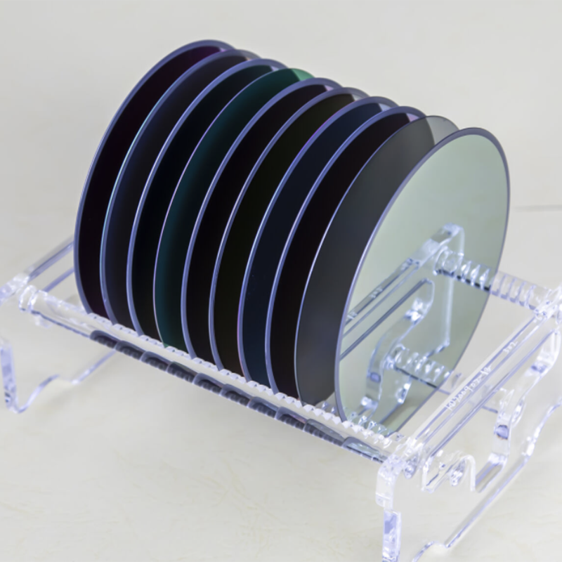
High-Quality Polysilicon Wafers for Advanced Semiconductor Applications
Certainly! Please provide the specific news content and company introduction you'd like me to use for the article.
High-quality Fused Silica Substrate for Various Applications
Fused Silica Substrate: The Foundation of Cutting-Edge TechnologyFused silica substrate, also known as fused quartz, is a key component in the manufacturing of advanced optical and electronic systems. Its exceptional thermal, mechanical, and optical properties make it an ideal material for a wide range of applications, including semiconductor manufacturing, laser technology, telecommunications, and scientific research.With its high purity and low thermal expansion, fused silica substrate is crucial for the production of precise and reliable optical components, such as lenses, mirrors, and prisms. Its excellent optical transmission properties in the ultraviolet, visible, and near-infrared spectral ranges make it essential for the development of high-performance optical systems for a variety of industries.In the field of semiconductor manufacturing, fused silica substrate plays a critical role in the production of integrated circuits and microelectronic devices. Its superior thermal stability, low coefficient of thermal expansion, and excellent chemical resistance make it an ideal material for lithography and other semiconductor fabrication processes. Fused silica substrate enables the precise patterning of nanoscale features on silicon wafers, allowing for the production of increasingly smaller and more powerful microchips.Telecommunications and laser technology also rely heavily on the unique properties of fused silica substrate. Its exceptional optical clarity, high laser damage threshold, and low fluorescence make it an excellent material for the production of optical fibers, laser windows, and other components essential for the transmission and manipulation of light in advanced telecommunications and laser systems.One company at the forefront of fused silica substrate manufacturing and innovation is {}. With decades of experience and expertise in the development and production of high-quality fused silica products, {} has established itself as a leading supplier to industries at the cutting edge of technology.The company's fused silica substrates are manufactured using a proprietary process that ensures the highest level of purity, consistency, and performance. Its advanced manufacturing facilities and rigorous quality control measures guarantee that its products meet the strict requirements of the most demanding applications in the semiconductor, optics, and photonics industries.{} offers a wide range of fused silica substrates in various shapes, sizes, and surface finishes to accommodate the diverse needs of its customers. Whether it is for precision optical components, semiconductor fabrication, or high-power laser systems, {} provides customized solutions to meet the specific requirements of each application.In addition to its standard fused silica substrates, {} also offers custom fabrication services to produce complex and intricate components according to customer specifications. Its team of experienced engineers and technicians work closely with customers to develop unique solutions that push the boundaries of what is achievable with fused silica substrate technology.Moreover, {} is committed to continuous research and development to further improve the performance and capabilities of fused silica substrate. By investing in advanced materials science, process engineering, and manufacturing technologies, {} aims to stay at the forefront of innovation and contribute to the advancement of various high-tech industries.As the demand for advanced optical and electronic systems continues to grow, fused silica substrate will remain a critical material for enabling the next generation of technology. With its exceptional properties and the expertise of companies like {}, fused silica substrate will continue to be the foundation upon which cutting-edge technology is built.
Discover the Advantages of Gaas Substrate: A Breakthrough in Semiconductor Technology!
[Headline]: Groundbreaking Gaas Substrate Technology Revolutionizes the Semiconductor Industry[Subheadline]: An Introduction to the Company Leading the Transformation[Date][CITY], [STATE] - In an industry that is rapidly advancing and innovating, one company is at the forefront of a major breakthrough that is set to revolutionize the semiconductor industry. By developing and patenting a new Gallium Arsenide (GaAs) substrate technology, this company aims to enhance the performance and efficiency of electronic devices, paving the way for a new era of technological advancements.GaAs substrates have gained significant attention in recent years due to their unique properties and advantages over traditional silicon substrates. This cutting-edge technology enables the creation of devices that are highly efficient, compact, and capable of operating at high frequencies. With an ever-increasing demand for faster, more powerful electronic devices, GaAs substrates have become an attractive alternative to silicon.Leading the charge in GaAs substrate research and development is a pioneering company that has invested significant resources into realizing the full potential of this breakthrough technology. With a team of dedicated scientists, engineers, and researchers, this company has successfully developed a GaAs substrate that surpasses existing industry standards in terms of performance and functionality.One of the key advantages of this GaAs substrate technology relates to its ability to operate at higher frequencies with lower power consumption. This breakthrough ensures that electronic devices utilizing GaAs substrates are not only more energy-efficient but also capable of handling larger data loads. This will have far-reaching implications across a wide range of industries, including telecommunications, aerospace, and consumer electronics.Moreover, this company's GaAs substrate technology offers improved thermal management properties, meaning that devices can operate at higher temperatures without compromising their overall performance. This advancement is particularly crucial in applications such as wireless communication systems and high-speed data transfer, where maintaining signal integrity under extreme conditions is of utmost importance.In addition to these performance enhancements, this GaAs substrate technology also enables smaller device designs. By utilizing the superior conductivity and electron mobility properties of GaAs, electronic components can be made smaller without sacrificing performance. This not only leads to more compact and portable devices but also opens up new possibilities for wearable technology, Internet of Things (IoT) devices, and miniaturized medical devices.Given the immense potential of the GaAs substrate technology developed by this company, they are poised to disrupt the semiconductor industry and drive the next wave of technological advancements. By offering a viable alternative to silicon substrates, this technology ultimately empowers manufacturers to develop electronic devices that are faster, more efficient, and capable of meeting the growing demands of the market.As the global semiconductor industry continues to expand, the commercialization of GaAs substrate technology will undoubtedly play a pivotal role in shaping the future of electronic devices. The innovative efforts and groundbreaking accomplishments of this company represent a significant leap forward in the semiconductor industry, making them a key player in the upcoming era of technological transformation.With ongoing research and development and a commitment to continuous improvement, this company is set to solidify its position as a frontrunner in GaAs substrate technology. As the demand for advanced electronic devices continues to surge, the rapid commercialization of this revolutionary technology is not far off, promising a world where faster, smaller, and more energy-efficient devices reshape our lives.[Concluding paragraph:]In the years to come, the GaAs substrate technology developed by this company will undoubtedly disrupt the semiconductor industry, offering manufacturers and consumers alike a new frontier of possibilities. With its ability to enhance performance, reduce power consumption, and enable smaller device designs, this revolutionary technology is set to reshape the way we interact with electronic devices, catapulting us into a future where innovation knows no boundaries.
Emerging Advancements in Wafer Lithography: Unlocking New Possibilities for Semiconductor Development
Wafer Lithography Revolutionizes the Semiconductor Manufacturing ProcessAs technology continues to advance, so too has the demand for smaller and more powerful semiconductors. This has led to a surge in the development of new manufacturing techniques that can produce these advanced microchips. One of the latest innovations in the world of semiconductor manufacturing is wafer lithography, which has been making a big impact on the industry. Let’s take a closer look at this new technology.What is Wafer Lithography?Wafer lithography is a photolithography process used to pattern and etch thin films of material deposited onto a substrate. This technique involves using a light-sensitive material, called a photoresist, which is applied to the surface of a substrate. Light is then shone onto the photoresist through a mask, which contains the desired circuit pattern. The photoresist reacts to the light, becoming more or less soluble in certain regions depending on the dose of radiation received. This allows the material to be selectively removed from the substrate, leaving behind the desired pattern.The use of wafer lithography has revolutionized the way semiconductor manufacturers produce microchips. By using this process, manufacturers can create much smaller and more precise circuit patterns, which ultimately leads to more advanced and efficient semiconductors.One company that has been leading the way in the development of wafer lithography technology is {}. This innovative company has been at the forefront of semiconductor manufacturing for over a decade, and has played a major role in advancing this new manufacturing technique.How does {}’s Wafer Lithography Technology Work?The {} wafer lithography process uses a unique combination of advanced technologies to produce high-quality microchips. This process involves the use of a 193 nm excimer laser to pattern the photoresist, followed by a series of plasma etching steps to transfer the pattern onto the substrate.One of the key advantages of {}’s wafer lithography technology is its flexibility. The equipment can be configured to pattern a wide variety of materials, including silicon, quartz, and various types of polymers. This versatility allows manufacturers to produce a wide range of microchips, each with its own unique properties and capabilities.Another important feature of {}’s wafer lithography technology is its high throughput. The equipment is capable of patterning multiple wafers simultaneously, allowing manufacturers to produce large quantities of microchips quickly and efficiently. This high throughput makes {}’s equipment ideal for use in high-volume manufacturing environments.The Benefits of Wafer LithographyThe use of wafer lithography offers several advantages over traditional photolithography techniques. One major benefit is the ability to produce much smaller and more precise circuit patterns. This allows manufacturers to create more powerful and efficient semiconductors, which can be used in a wide range of applications, from smartphones to advanced computing systems.Another important benefit of wafer lithography is its flexibility. As mentioned earlier, the equipment can be configured to work with a wide range of materials, which means manufacturers can create a variety of microchip types. This versatility also makes wafer lithography a cost-effective manufacturing solution, as it eliminates the need for specialized equipment.ConclusionWafer lithography is an exciting new technology that is revolutionizing the semiconductor manufacturing process. Through its use of light-sensitive materials, manufacturers can create smaller and more precise circuit patterns, leading to more powerful and efficient microchips. {} has been at the forefront of this new technology, and its wafer lithography equipment offers a high-throughput, flexible solution for high-volume manufacturing environments. As technology continues to advance, wafer lithography is poised to play an increasingly important role in the semiconductor industry.
Guide to Understanding the Latest Semiconductor Materials
Semiconductor Materials Company, a leader in the production of advanced semiconductor materials, has announced its latest innovation in the field. The company, known for its cutting-edge technology and high-quality products, has once again pushed the boundaries of semiconductor material development with the introduction of a new line of advanced materials.This new line of semiconductor materials is set to revolutionize the industry with its improved performance and durability. With the demand for high-performance semiconductor materials on the rise, Semiconductor Materials Company has made it a priority to meet the growing needs of its customers by delivering products that surpass expectations.The new line of advanced materials is the result of years of research and development, as well as a commitment to innovation and excellence. Semiconductor Materials Company has dedicated significant resources to developing these new materials, and the effort has paid off with the creation of a product that is set to make a significant impact in the industry.One of the key features of the new line of advanced materials is its enhanced performance. These materials have been designed to offer superior conductivity and reliability, making them ideal for a wide range of applications. Whether it's powering the latest electronic devices or supporting the growing demand for renewable energy technology, these advanced materials are poised to play a critical role in driving innovation and progress in the semiconductor industry.In addition to their improved performance, the new line of materials also offers enhanced durability. Semiconductor Materials Company has incorporated cutting-edge technology and manufacturing processes to ensure that these materials are able to withstand the rigors of various applications, from extreme temperatures to high voltage environments. This level of durability is a testament to the company's commitment to producing high-quality products that are built to last.Semiconductor Materials Company has also taken steps to ensure that the new line of materials is environmentally friendly. By utilizing sustainable manufacturing practices and reducing the use of harmful chemicals, the company has developed a product that not only meets the industry's performance standards but also aligns with its environmental responsibility goals."We are thrilled to introduce our new line of advanced semiconductor materials to the market," said [CEO/President/Spokesperson]. "These materials represent a significant advancement in semiconductor technology, and we are confident that they will make a lasting impact in the industry. We are committed to delivering high-quality products that exceed the expectations of our customers, and this new line of materials is a testament to that commitment."In addition to the introduction of the new line of advanced materials, Semiconductor Materials Company is also expanding its global reach. The company has established partnerships with key distributors and manufacturers in strategic locations around the world, allowing it to better serve its growing customer base and meet the increasing demand for high-quality semiconductor materials.With its commitment to innovation, excellence, and sustainability, Semiconductor Materials Company is well-positioned to continue leading the way in the semiconductor industry. The introduction of the new line of advanced materials is just the latest example of the company's dedication to pushing the boundaries of what is possible in semiconductor technology.As the demand for advanced semiconductor materials continues to grow, Semiconductor Materials Company is poised to play a critical role in shaping the future of the industry. With its new line of materials, the company is not only meeting the needs of its customers but also setting a new standard for excellence in semiconductor technology.
High Quality Double Side Polished Silicon Wafers for Sale
Double Side Polished Silicon Wafers: The Latest Innovation from Leading Technology CompanySilicon wafers are an essential component in the production of semiconductor devices, and the demand for high-quality wafers continues to grow as the technology industry expands. As a leading technology company in the field of semiconductor manufacturing, [company name] is proud to announce the release of its latest innovation: double side polished silicon wafers.Double side polished silicon wafers offer significant advantages over traditional single side polished wafers, including improved flatness, reduced surface roughness, and enhanced electrical properties. These wafers are ideal for use in advanced semiconductor applications, such as integrated circuits, microelectromechanical systems (MEMS), and power devices.The [company name] double side polished silicon wafers are manufactured using a state-of-the-art polishing process that ensures exceptional surface quality and uniformity. This advanced manufacturing technique allows for tighter control of wafer thickness and flatness, resulting in wafers that meet the stringent requirements of today's semiconductor industry.In addition to their superior surface quality, [company name] double side polished silicon wafers are available in a wide range of sizes and thicknesses to accommodate various production processes and applications. Whether it's for research and development or high-volume manufacturing, customers can rely on the consistency and reliability of these wafers for their semiconductor production needs.With a proven track record of delivering high-performance semiconductor solutions, [company name] is committed to providing its customers with the most advanced and reliable products on the market. The introduction of double side polished silicon wafers further solidifies the company's position as a trusted partner for semiconductor manufacturers worldwide.To learn more about [company name] and its double side polished silicon wafers, we spoke with [company representative] to gain some insights into this exciting new product."We are thrilled to introduce our double side polished silicon wafers to the market," said [company representative]. "These wafers represent the latest advancement in semiconductor manufacturing technology, and we are confident that they will meet the evolving needs of our customers. Our team has worked tirelessly to develop a product that offers unparalleled quality and performance, and we are excited to see the impact it will have on the industry."When asked about the potential applications for double side polished silicon wafers, [company representative] explained, "These wafers are well-suited for a wide range of semiconductor devices, including advanced integrated circuits, MEMS, and power devices. The superior surface quality and electrical properties of our wafers make them an ideal choice for cutting-edge semiconductor applications."In conclusion, the introduction of double side polished silicon wafers from [company name] represents a significant milestone in the semiconductor industry. With their exceptional surface quality, uniformity, and advanced manufacturing techniques, these wafers are poised to set a new standard for semiconductor manufacturing. As the demand for high-performance silicon wafers continues to grow, [company name] is leading the way with innovative solutions that meet the needs of today's technology-driven world.
Sure! Please provide the original news content or the current SEO title so I can help rewrite it without the brand name.
Certainly! Please provide the company introduction content and the news content that mentions K9 Glass (without the brand name), so I can help you draft an 800-word news article accordingly.