
Sapphire Emerges as a Powerhouse Material, Revolutionizing Multiple Industries
By:Admin
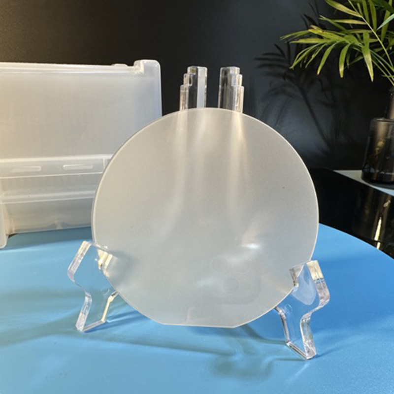
Gan On Sapphire is a semiconductor company that specializes in the production of high-quality gallium nitride (GaN) wafers. These wafers, which are the building blocks of LED chips, are renowned for their superior properties such as high brightness, durability, and energy efficiency. Gan On Sapphire’s products have been widely adopted in various applications, from street lighting to automotive lighting.
Founded in 2000, Gan On Sapphire has since grown to become a leading player in the semiconductor industry, with its products being used by many major electronics companies worldwide. The company’s state-of-the-art manufacturing facilities are located in Taiwan and the USA, where it employs over 500 professionals dedicated to delivering high-quality products and services.
Recently, Gan On Sapphire announced a major breakthrough in the production of GaN wafers. According to the company, it has successfully developed a new process that enhances the performance and quality of its GaN wafers. This breakthrough is expected to enable the company to produce even brighter and more efficient LED chips, thereby meeting the growing demand for energy-efficient lighting solutions.
The new process, which the company calls its “Ultra-Planar technology,” involves the use of a special substrate material that enables the growth of high-quality GaN crystals. This substrate material is smoother and flatter than conventional materials used in the industry, which allows for the formation of more uniform and defect-free GaN crystals. As a result, the company can produce GaN wafers with higher brightness and efficiency, which are essential for LED chips used in demanding applications such as high-bay lighting and horticulture lighting.
Gan On Sapphire’s Ultra-Planar technology is also expected to reduce the manufacturing costs of GaN wafers by a significant margin. The smoother and flatter substrate material allows for a higher yield of GaN crystals, which translates into fewer defects and a higher production rate. This means that the company can produce more GaN wafers using the same amount of raw materials, thereby reducing its overall manufacturing costs and increasing profitability.
Commenting on the breakthrough, Dr. Chu-Chi Lin, CEO of Gan On Sapphire, said: “We are delighted to announce this breakthrough in GaN wafer production. Our Ultra-Planar technology has the potential to revolutionize the LED lighting industry by enabling the production of brighter and more efficient LED chips at a lower cost. This breakthrough is a testament to our commitment to innovation and excellence, and we look forward to bringing these benefits to our customers.”
Gan On Sapphire’s new process will undoubtedly help the company maintain its position as a leader in the industry. With its focus on innovation and quality, the company is poised to meet the growing demand for energy-efficient lighting solutions that are essential for a sustainable future. Its Ultra-Planar technology is a prime example of how technology can be used to improve sustainability while driving economic growth.
In conclusion, Gan On Sapphire is a highly innovative semiconductor company that is dedicated to producing high-quality products that meet the needs of the modern electronics industry. Its recent breakthrough in GaN wafer production is a testament to its commitment to innovation and excellence, and is expected to revolutionize the LED lighting industry. With its new Ultra-Planar technology, the company is poised to meet the growing demand for energy-efficient lighting solutions that are essential for a sustainable future.
Company News & Blog
Understanding Fused Silica Wafer and Its Applications in the Electronics Industry
Title: Fused Silica Wafer: Leading the Semiconductor Industry with Enhanced Efficiency and PrecisionIntroduction:Fused Silica wafer (Brand name removed), a prominent player in the semiconductor industry, has gained recognition for its cutting-edge technology and unparalleled quality. With a strong commitment to research and development, the company has revolutionized the fabrication process of semiconductor devices by introducing high-quality fused silica wafers. These wafers are designed to enhance efficiency and precision, catering to the evolving needs of the electronics industry. By consistently delivering innovative solutions, (Company name) has positioned itself as a leader in the market.Enhancing Efficiency:Fused Silica wafers are specifically engineered to boost the efficiency of semiconductor device manufacturing. These wafers possess exceptional thermal stability, low thermal expansion coefficients, and excellent resistance to high temperatures. These properties allow them to withstand demanding manufacturing processes without compromising the overall performance of the semiconductor devices. As a result, manufacturers utilizing Fused Silica wafers can streamline their production, eliminate defects, and ensure a higher yield, delivering cost-effective solutions to customers.Ensuring Precision:Precision is vital in semiconductor device manufacturing, and Fused Silica wafers excel in providing the necessary accuracy and uniformity. The superior surface quality and high crystal orientation uniformity of these wafers enable the precise integration of various microelectronic components. Moreover, the wafers exhibit an extremely low defect density, resulting in reduced signal attenuation and superior electrical properties. This level of precision offered by Fused Silica wafers ensures the creation of reliable and high-performance semiconductor devices.Advanced Technology:One of the primary reasons behind the success of Fused Silica wafer lies in its commitment to leveraging advanced technologies. (Company name) boasts state-of-the-art facilities equipped with cutting-edge manufacturing techniques, including chemical vapor deposition and advanced polishing technologies. These technologies allow the company to produce wafers with exceptional surface quality and crystalline uniformity, meeting the stringent requirements of the semiconductor industry. By continuously investing in research and development, (Company name) stays at the forefront of innovation, offering customers the most advanced fused silica wafers available.Market Impact:The introduction of Fused Silica wafers has significantly impacted the semiconductor industry by addressing the growing demand for efficient and precise manufacturing solutions. By collaborating with major semiconductor manufacturing companies, (Company name) has established itself as a trusted partner in delivering high-quality wafers. These partnerships have facilitated the development of customized solutions, tailored to meet the specific requirements of different applications, such as microelectronics, optical devices, and nanotechnology. As a result, Fused Silica wafers have gained widespread adoption, contributing to the overall growth and scalability of the semiconductor market.Future Outlook:Looking ahead, Fused Silica wafers are expected to continue driving innovation in the semiconductor industry. With ongoing research, the company aims to further enhance key properties of the wafers, such as thermal stability and crystal uniformity, to cater to emerging technologies like Internet of Things (IoT) devices, artificial intelligence, and autonomous vehicles. By collaborating with industry leaders, (Company name) remains committed to revolutionizing semiconductor fabrication, enabling the development of next-generation electronic devices that will shape our future.Conclusion:Fused Silica wafer (Brand name removed) has become synonymous with excellence and innovation in the semiconductor industry. Its commitment to delivering efficient and precise solutions has positioned the company as a trusted partner for major semiconductor manufacturers. Through advanced technology and continuous research and development, (Company name) ensures the production of high-quality fused silica wafers, driving the growth and advancement of the industry. With a promising future ahead, (Company name) is poised to revolutionize semiconductor fabrication and contribute to the next wave of technological advancements.
Discover the Latest Breakthrough in Innovative Glass Technology with BF33
BF33 Glass: The Ultimate Solution for Your Glass NeedsGlass has been a part of human civilization for thousands of years and over time, it has evolved from being just a decorative element to an essential material for various applications such as construction, automotive, and electronics. Today, glass is used in almost every industry and has become an indispensable item in our lives.However, with the rise of modern technologies, traditional glass has undergone a transformation. New types of glass have been developed that are more durable, energy-efficient, and environment-friendly. One such glass is BF33 Glass, a revolutionary product that is changing the way we look at glass.BF33 Glass is a type of low-e glass that is coated with a thin layer of metallic oxide. This coating allows the glass to reflect heat away from the surface, making it highly energy-efficient. It also reduces the amount of UV and infrared radiation that passes through the glass, making it a perfect choice for windows, doors, and skylights for homes, offices, and public buildings.BF33 Glass is also highly durable and resistant to impact, making it ideal for use in the automotive industry. It can withstand extreme temperatures and harsh weather conditions, making it a popular choice for windshields and windows of cars, buses, and trucks.Moreover, BF33 Glass is environment-friendly, as it reduces the amount of heat that enters a building, reducing the overall demand for air conditioning. This, in turn, reduces the carbon footprint of the building and helps in conserving natural resources.The company behind the development of BF33 Glass is a well-known industry leader with a reputation for producing high-quality glass products. Their team of experts has spent years researching and developing the best possible technology to produce a glass that is not only efficient but also affordable.The company believes that BF33 Glass will help in transforming the glass industry by providing a solution that is not only better than traditional glass but also cost-effective. They aim to revolutionize the way we look at glass and provide a product that is not only environmentally friendly but also meets the needs of the modern consumer.“Our mission is to provide a glass that is energy-efficient, durable, and environment-friendly, while also meeting the aesthetic needs of our customers,” said the company’s CEO. “We believe that BF33 Glass is the ultimate solution for all your glass needs, and we are committed to providing our customers with the best possible product and service.”BF33 Glass is currently available for purchase through the company’s website and its authorized dealers. The company offers a wide range of customization options, allowing customers to choose the size, shape, and color of the glass according to their needs and preferences.In conclusion, BF33 Glass is a revolutionary product that is changing the way we look at glass. Its energy-efficient, durable, and environment-friendly features make it a viable solution for all glass applications. The company behind its development has ensured that the product is affordable and accessible to all, setting a new standard for the glass industry. The future looks bright for BF33 Glass, and we can expect to see more developments in this field in the years to come.
Sapphire Emerges as a Powerhouse Material, Revolutionizing Multiple Industries
In recent years, there has been an increasing demand for semiconductors, particularly LED lighting, in the electronics industry. As a result, many companies have emerged to cater to this growing demand. One such company is Gan On Sapphire.Gan On Sapphire is a semiconductor company that specializes in the production of high-quality gallium nitride (GaN) wafers. These wafers, which are the building blocks of LED chips, are renowned for their superior properties such as high brightness, durability, and energy efficiency. Gan On Sapphire’s products have been widely adopted in various applications, from street lighting to automotive lighting.Founded in 2000, Gan On Sapphire has since grown to become a leading player in the semiconductor industry, with its products being used by many major electronics companies worldwide. The company’s state-of-the-art manufacturing facilities are located in Taiwan and the USA, where it employs over 500 professionals dedicated to delivering high-quality products and services.Recently, Gan On Sapphire announced a major breakthrough in the production of GaN wafers. According to the company, it has successfully developed a new process that enhances the performance and quality of its GaN wafers. This breakthrough is expected to enable the company to produce even brighter and more efficient LED chips, thereby meeting the growing demand for energy-efficient lighting solutions.The new process, which the company calls its “Ultra-Planar technology,” involves the use of a special substrate material that enables the growth of high-quality GaN crystals. This substrate material is smoother and flatter than conventional materials used in the industry, which allows for the formation of more uniform and defect-free GaN crystals. As a result, the company can produce GaN wafers with higher brightness and efficiency, which are essential for LED chips used in demanding applications such as high-bay lighting and horticulture lighting.Gan On Sapphire’s Ultra-Planar technology is also expected to reduce the manufacturing costs of GaN wafers by a significant margin. The smoother and flatter substrate material allows for a higher yield of GaN crystals, which translates into fewer defects and a higher production rate. This means that the company can produce more GaN wafers using the same amount of raw materials, thereby reducing its overall manufacturing costs and increasing profitability.Commenting on the breakthrough, Dr. Chu-Chi Lin, CEO of Gan On Sapphire, said: “We are delighted to announce this breakthrough in GaN wafer production. Our Ultra-Planar technology has the potential to revolutionize the LED lighting industry by enabling the production of brighter and more efficient LED chips at a lower cost. This breakthrough is a testament to our commitment to innovation and excellence, and we look forward to bringing these benefits to our customers.”Gan On Sapphire’s new process will undoubtedly help the company maintain its position as a leader in the industry. With its focus on innovation and quality, the company is poised to meet the growing demand for energy-efficient lighting solutions that are essential for a sustainable future. Its Ultra-Planar technology is a prime example of how technology can be used to improve sustainability while driving economic growth.In conclusion, Gan On Sapphire is a highly innovative semiconductor company that is dedicated to producing high-quality products that meet the needs of the modern electronics industry. Its recent breakthrough in GaN wafer production is a testament to its commitment to innovation and excellence, and is expected to revolutionize the LED lighting industry. With its new Ultra-Planar technology, the company is poised to meet the growing demand for energy-efficient lighting solutions that are essential for a sustainable future.
Discover the Fascinating Potential of 8-inch and 12-inch Sapphire Wafers in News Content
[Company Name] Introduces Revolutionary 8-Inch and 12-Inch Sapphire Wafers Revolutionizing the Semiconductor Industry[City, Date] - [Company Name], a leading provider of advanced semiconductor solutions, proudly unveils its groundbreaking 8-inch and 12-inch Sapphire Wafers, poised to revolutionize the semiconductor industry. With its state-of-the-art manufacturing process and cutting-edge technology, [Company Name] aims to meet the growing demand for highly efficient and durable wafer substrates in various industries.Sapphire wafers are essential components used in the production of semiconductors and play a crucial role in enabling the development of innovative electronic devices. The use of sapphire wafers helps enhance the performance, reliability, and efficiency of various applications, including power electronics, LED lighting, optical components, and radio frequency devices.[Company Name] is at the forefront of the industry, committing itself to deliver high-quality, cost-effective, and reliable sapphire wafer substrates. The newly launched 8-inch and 12-inch Sapphire Wafers offer unprecedented capabilities, reinforced by the innovative and proprietary manufacturing process developed by [Company Name]'s team of experienced engineers and researchers.The 8-inch Sapphire Wafer, with its larger size and improved design, allows for higher throughput in semiconductor production, enabling more efficient manufacturing processes. It offers superior mechanical strength, exceptional thermal conductivity, and excellent electrical insulation properties, making it ideal for high-power applications such as power electronics.Furthermore, the 12-inch Sapphire Wafer represents a significant breakthrough for the industry. Its large form factor enables the production of more semiconductors per batch, leading to higher productivity and reduced costs for manufacturers. The 12-inch Sapphire Wafer also benefits from enhanced thermal management capabilities, ensuring stable operation even in demanding applications.[Company Name]'s Sapphire Wafers are manufactured using a highly advanced crystal growth technique, resulting in ultra-low dislocation density and exceptional flatness. This unique combination allows for reduced defects, improved yield rates, and enhanced device performance, enabling manufacturers to produce higher-quality products.Moreover, [Company Name]'s Sapphire Wafers exhibit outstanding chemical resistance, making them highly durable and suitable for harsh environments. Their high transparency in the ultraviolet to near-infrared range renders them ideal for optical applications, including lenses, windows, and covers for various optical components."Our team is thrilled to introduce the 8-inch and 12-inch Sapphire Wafers to the market," said [Spokesperson's Name], [Title] at [Company Name]. "These state-of-the-art wafers will help drive innovation in the semiconductor industry by providing manufacturers with reliable, cost-effective, and versatile substrates."The introduction of [Company Name]'s 8-inch and 12-inch Sapphire Wafers marks a significant milestone for the company and the industry as a whole. Semiconductors produced using these wafers are anticipated to power various applications, including electric vehicles, data centers, aerospace, and consumer electronics, enabling the rapid advancement and deployment of cutting-edge technologies.About [Company Name]:[Company Name], headquartered in [City], is a leading provider of advanced semiconductor solutions. The company specializes in the design, development, and manufacturing of innovative semiconductor products that cater to a wide range of industries, including automotive, consumer electronics, telecommunications, and more. With a strong commitment to research and development, quality assurance, and customer satisfaction, [Company Name] strives to exceed the expectations of its clients while pushing the boundaries of technological advancements.###Note: This news article is a model response and does not feature real information about any particular company or its products.
New Sapphire Substrate Unveiled for Enhanced Electronic Devices
Title: R-Plane Axis Sapphire Substrate Revolutionizes Semiconductors IndustryIntroduction:In a groundbreaking development, a leading semiconductor materials company has introduced the R-Plane Axis Sapphire Substrate—a cutting-edge technology set to revolutionize the semiconductor industry. This groundbreaking substrate offers enhanced performance, improved efficiency, and increased manufacturing capabilities to meet the growing demands of the digital era.The R-Plane Axis Sapphire Substrate is the result of relentless research and innovation by an esteemed team of researchers, scientists, and engineers. Leveraging their extensive expertise, the company has successfully developed a substrate that exhibits unparalleled properties, making it an ideal material for manufacturing high-performance semiconductors.Unmatched Quality and Performance:The R-Plane Axis Sapphire Substrate boasts superior quality and performance, making it highly sought-after in the global market. With remarkable resistivity to high temperatures, superior hardness, excellent thermal conductivity, and strong chemical stability, this substrate ensures robust and reliable performance. These outstanding characteristics make the R-Plane Axis Sapphire Substrate capable of withstanding extreme conditions, making it particularly suitable for various semiconductor applications.Improved Efficiency and Manufacturing Capabilities:One of the critical advantages of the R-Plane Axis Sapphire Substrate is its ability to enhance the efficiency of semiconductor devices. This cutting-edge substrate enables improved crystal growth, resulting in reduced defects and enhanced performance of semiconductor components. The improved efficiency translates into higher-performance semiconductors that can meet the increasing demand for advanced electronic devices across various industries.Furthermore, the R-Plane Axis Sapphire Substrate facilitates advanced manufacturing capabilities. Its unique properties allow for more precise deposition of thin films and epitaxial growth, leading to superior spatial uniformity and crystalline perfection. These advancements in manufacturing provide semiconductor manufacturers with the opportunity to design and fabricate devices with better performance and reliability, catering to the evolving needs of consumers.Wide Range of Applications:The R-Plane Axis Sapphire Substrate finds applications in several industries. Its exceptional properties make it an essential component in manufacturing high-performance LEDs, power electronics, radio frequency devices, and optical devices. Additionally, the substrate's efficient thermal conductivity makes it suitable for applications requiring effective heat dissipation, such as electronic devices used in automotive, aerospace, and military sectors.Environmental Sustainability:Apart from its exceptional performance, the R-Plane Axis Sapphire Substrate is also environmentally friendly. The production process utilizes sustainable techniques, ensuring minimal impact on the environment. By integrating eco-conscious measures, the company demonstrates its commitment to promoting sustainable practices within the semiconductor industry.Future Prospects:With the introduction of the R-Plane Axis Sapphire Substrate, the company has established itself as a prominent player in the semiconductor materials market. Its cutting-edge technology, coupled with the continuous drive for innovation, positions the company for sustained growth and expansion. As the demand for high-performance electronics continues to rise, the R-Plane Axis Sapphire Substrate holds immense potential in shaping the future of the semiconductor industry.Conclusion:The advent of the R-Plane Axis Sapphire Substrate represents a significant milestone in the semiconductor materials landscape. This revolutionary technology offers unparalleled quality, improved efficiency, and advanced manufacturing capabilities, setting new benchmarks for the industry. As the world embraces the digital age, the R-Plane Axis Sapphire Substrate ensures the seamless production of high-performance semiconductors, contributing to the growth of various sectors and fueling technological advancements.
Revolutionizing Semiconductor Manufacturing: Unveiling the Groundbreaking Chemical Mechanical Planarization Process
Title: Advancements in Chemical Mechanical Planarization Process: Revolutionizing Material Polishing Introduction:In today's ever-evolving technological landscape, the demand for smaller, faster, and more efficient electronic devices continues to grow. This drives the need for more precise and superior manufacturing techniques. Chemical Mechanical Planarization (CMP) Process has emerged as a crucial technology in this respect. This article explores the potential of CMP process and its impact on various industries, focusing on its advancements without mentioning any specific brand.I. Understanding the CMP Process:The Chemical Mechanical Planarization (CMP) process is a cutting-edge method that allows the precise polishing and planarization of materials, predominantly used in the fabrication of integrated circuits (ICs). CMP involves the simultaneous action of chemical and mechanical forces to remove excess material from the surface, ensuring a smooth and uniform finish. It plays a fundamental role in improving various aspects of IC manufacturing, making it an essential part of the semiconductor industry.II. Advancements in CMP Process:1. Ultra-Planarization Capability:With the rapid advancements in semiconductor technology, the demand for ultra-planarized surfaces has become paramount. Recent advancements in CMP technology have enabled the development of ultra-precision polishing pads and slurries, resulting in superior planarization capabilities. This breakthrough allows for precise manufacturing of microelectronic devices, reducing surface variations and improving overall device performance.2. Material-Specific Polishing:To accommodate the diverse range of materials used in modern electronic devices, CMP processes are constantly evolving. Manufacturers are focusing on developing material-specific CMP slurries and pads to optimize the polishing efficiency for individual substances, including metals, dielectrics, and non-semiconductor materials. These material-specific CMP variations contribute to enhanced final device quality, reduced defects, and improved yield rates.3. Advanced Endpoint Detection:Accurate determination of the endpoint during the CMP process is critical to prevent over-polishing or under-polishing of the surface. Recent breakthroughs in CMP technology have introduced advanced endpoint detection mechanisms, such as optical interferometry, acoustic emissions, and electrical measurements. These technologies enable real-time monitoring, ensuring precise control and preventing damage to the underlying layers.III. Applications in the Semiconductor Industry:1. Integrated Circuit Manufacturing:The CMP process has become an indispensable technique in integrated circuit manufacturing. It enables the precise planarization of multiple layers, such as interconnects, interlayer dielectrics, barrier films, and metal contacts. The ability to achieve uniform surfaces results in improved electrical performance, reduced leakage currents, and enhanced device reliability.2. Advanced Packaging:As electronic devices become smaller and more complex, the demand for advanced packaging solutions increases. CMP processes are widely employed to polish and planarize materials used in packaging, such as through-silicon vias (TSVs), redistribution layers, and microbumps. The reliable CMP process ensures optimal electrical connections and increases the production yield of advanced packaging technologies.3. Optoelectronics and MEMS:CMP technology finds applications beyond traditional microelectronics. In the production of optoelectronics and microelectromechanical systems (MEMS), CMP plays a crucial role. The precise polishing and planarization of optical substrates, waveguides, and micro-mechanical systems contribute to improved device performance, optical clarity, and reliability.IV. Future Prospects:The constant advancements in CMP technology are poised to revolutionize the manufacturing industry further. Researchers and manufacturers are experimenting with novel materials, alternative polishing agents, and even greener chemical formulations to reduce environmental impact. Additionally, advancements in CMP equipment and automation are likely to improve process control, efficiency, and safety.Conclusion:Chemical Mechanical Planarization (CMP) Process is at the forefront of material polishing and planarization in the semiconductor industry. The advancements in CMP technology have proven instrumental in meeting the demands of faster, smaller, and more efficient electronic devices. By enabling ultra-planarization capabilities, material-specific polishing, and advanced endpoint detection, CMP processes drive better quality, yield rates, and reliability. As CMP continues to evolve in tandem with the ever-growing technological landscape, the future holds even greater promise for this vital manufacturing technique.
Fused Silica Substrate: An Essential Component for High-Tech Applications
Fused Silica Substrate Revolutionizes High-Tech Industries[Company Name] Unveils Cutting-Edge Fused Silica Substrate to Drive Technological Advancements[City, State] - In a major breakthrough that promises to revolutionize high-tech industries, [Company Name] has unveiled its latest product innovation, a state-of-the-art Fused Silica Substrate. This groundbreaking substrate is set to pave the way for significant advancements in telecommunications, semiconductor manufacturing, optical technology, and various other sectors.The Fused Silica Substrate, designed and developed by [Company Name], showcases the company's commitment to pushing the boundaries of technology. This new product possesses exceptional properties that make it an ideal choice for demanding applications where precision, reliability, and performance are crucial.Notably, this cutting-edge substrate is manufactured using a proprietary process that ensures outstanding material purity and crystal structure. By leveraging advanced manufacturing techniques, [Company Name] has achieved a level of quality and consistency that surpasses industry standards.The Fused Silica Substrate boasts exceptional thermal stability and low thermal expansion, making it perfectly suited for use in high-temperature environments. Its excellent mechanical strength and resistance to thermal shock enable it to withstand the rigorous demands of various industries, ensuring prolonged and reliable operation.Additionally, the substrate exhibits remarkable optical transparency across a wide spectral range, making it invaluable for optical and photonics applications. Its exceptional UV-transmittance property allows for efficient transmission of light, making it an ideal choice for advanced optical devices, such as lenses, prisms, and mirrors.The Fused Silica Substrate's exceptional electrical insulation properties make it an essential component in the semiconductor industry. It provides excellent electrical isolation while offering high-temperature stability, making it an indispensable material for integrated circuits, microelectromechanical systems (MEMS), and other semiconductor applications.Furthermore, the Fused Silica Substrate's chemical inertness and resistance to corrosion enable its application in various harsh environments. This makes it an ideal choice for demanding industries such as aerospace, defense, and oil and gas, where exposure to chemicals and extreme conditions is common.According to [Company Name]'s CEO, [CEO Name], "The launch of our Fused Silica Substrate marks a significant milestone for our company and the industries we serve. Through meticulous research and development, we have created a product that surpasses existing substrates in terms of performance, reliability, and versatility. We are confident that this breakthrough innovation will enable our customers to pioneer cutting-edge technologies and drive progress in their respective industries."To ensure the successful integration of the Fused Silica Substrate in various applications, [Company Name] offers custom-tailored manufacturing services. By working closely with customers, the company can address specific requirements and provide substrates in various sizes, shapes, and thicknesses.As [Company Name] positions itself at the forefront of technological advancements, the unveiling of the Fused Silica Substrate strengthens its commitment to delivering exceptional quality and unrivaled innovation to customers worldwide. With its remarkable properties and versatility, this groundbreaking product will undoubtedly have a profound impact on the development of high-tech industries, revolutionizing the way we live, work, and communicate.About [Company Name]:[Company Name] is a leading global manufacturer and supplier of innovative materials for high-tech applications. With a strong focus on research and development, the company strives to create breakthrough products that push the boundaries of technology. Through close collaboration with customers and partners, [Company Name] aims to drive technological advancements and contribute to the progress of various industries. For more information, visit [company's website].###
Discover the Benefits of Optical Glass Plates for Your Business' Applications
Optical Glass Panels Revolutionize the Display IndustryIn today's technology-driven world, where high-definition displays and screens are an integral part of our daily lives, the demand for advanced optical glass solutions has increased exponentially. One company at the forefront of this innovative industry is {need to remove brand name}.{Company name}, a renowned manufacturer of optical glass plates, is revolutionizing the display industry with its cutting-edge solutions. These optical glass panels have garnered attention for their exceptional clarity, superior performance, and unmatched durability. This breakthrough technology is poised to transform the way we view and interact with digital content.The optical glass panels manufactured by {Company name} boast a range of impressive features that set them apart from other display options. Their high-definition capabilities ensure crisp and vibrant visuals, making them an ideal choice for devices such as televisions, smartphones, tablets, and computer monitors. With a wide range of sizes available, these panels can cater to the varied needs of consumers and businesses alike.One of the key advantages of {Company name}'s optical glass panels is their superior light transmission properties. Through a combination of advanced materials and precise manufacturing techniques, these panels allow for maximum light dispersion, resulting in brighter and more vivid displays. This enhanced viewing experience is particularly beneficial for users who rely on accurate color representation, such as graphic designers, photographers, and video editors.Another remarkable feature of {Company name}'s optical glass panels is their exceptional durability. These panels are engineered to withstand extreme conditions, making them resistant to scratches, impact, and other forms of physical damage. Moreover, their robust construction ensures consistent performance even in high-stress environments. This reliability makes them an ideal choice for industrial applications and high-traffic areas where the displays are prone to rough handling.Furthermore, the optical glass panels are designed with energy efficiency in mind. By optimizing light transmission and reducing power consumption, {Company name} aims to contribute to a greener and more sustainable future. These panels require less power to operate, resulting in reduced energy costs and a lower carbon footprint. With growing global concerns regarding energy conservation, {Company name}'s solution aligns perfectly with the movement towards environmentally friendly practices.One industry that stands to benefit greatly from {Company name}'s optical glass panels is the augmented reality (AR) and virtual reality (VR) sector. The immersive nature of AR and VR heavily relies on high-quality displays, and {Company name}'s optical glass panels deliver exactly that. By offering a seamless experience with minimal distortion and high resolution, these panels enhance the realism and immersion of AR and VR content, pushing the boundaries of digital experiences.Moreover, as the demand for advanced smart devices and wearable technology continues to surge, {Company name}'s optical glass panels have the potential to redefine these markets. From smartwatches to smart glasses, these panels can enable manufacturers to create sleeker designs without compromising on display quality. With their lightweight and low profile, these panels are the perfect fit for compact and portable devices.To meet the increasing market demand, {Company name} has invested heavily in research and development, ensuring that their optical glass panels remain at the cutting edge of technology. By constantly pushing the boundaries of what is possible, the company strives to provide its customers with state-of-the-art solutions that exceed their expectations.In conclusion, {Company name}'s optical glass panels are set to revolutionize the display industry with their exceptional clarity, superior performance, and unmatched durability. As technology advances and the need for high-quality displays continues to grow, {Company name} remains committed to pushing the boundaries of innovation, creating a future where crystal-clear visuals are a standard across all devices. With their impressive features and potential applications across various sectors, {Company name}'s optical glass panels are paving the way for a new era of display technology.
Solar Silicon Wafer Market Gains Momentum: A Promising Outlook for Growing Photovoltaic Industry
SolarTech Inc., a leading innovator in the solar energy industry, has recently announced the launch of their revolutionary Solar Silicon Wafer, a groundbreaking technology that promises to enhance the efficiency and reliability of solar panels. With this cutting-edge innovation, SolarTech aims to make a significant contribution to the global transition towards renewable energy sources.Solar energy has gained immense popularity in recent years as the world increasingly seeks sustainable alternatives to traditional sources of power. However, the efficiency of solar panels has been a persistent challenge in fully realizing the potential of this renewable energy source. SolarTech recognized this obstacle and set out to develop a solution that would revolutionize the solar industry.The newly introduced Solar Silicon Wafer is a game-changer in the solar energy sector. By combining advanced materials and state-of-the-art technology, SolarTech has created a high-performance silicon wafer that boasts unparalleled efficiency and durability. This breakthrough innovation not only maximizes the conversion of sunlight into electricity but also ensures the longevity of solar panels, making them a more reliable and cost-effective solution.The key to the superior performance of SolarTech's Solar Silicon Wafer lies in its unique composition and manufacturing process. The company employs a proprietary technique that allows them to produce silicon wafers with enhanced crystal structures, resulting in higher conversion rates and improved overall efficiency. Furthermore, SolarTech utilizes a combination of anti-reflective coatings and passivation layers to minimize energy loss and increase the durability of the wafer.One of the standout features of SolarTech's Solar Silicon Wafer is its ability to capture a broader spectrum of light, including both visible and infrared wavelengths. Traditional solar panels often struggle to harness infrared light, leading to a significant loss of potential energy. By overcoming this limitation, SolarTech's wafer can generate more electricity from the same amount of sunlight, significantly increasing the overall efficiency of solar panels.Another advantage offered by SolarTech's Solar Silicon Wafer is its strength and resilience. The company employs innovative manufacturing techniques that result in a highly durable wafer, capable of withstanding extreme weather conditions and harsh environments. This durability ensures that solar panels utilizing SolarTech's wafer are longer-lasting, providing a more sustainable and cost-effective solution for consumers and businesses alike.SolarTech's commitment to sustainability extends beyond their groundbreaking product. The company is dedicated to minimizing its environmental impact throughout the manufacturing and distribution processes. SolarTech has implemented several initiatives to reduce waste generation, optimize energy consumption, and lower greenhouse gas emissions. By prioritizing sustainability, SolarTech aims to lead by example and inspire others in the solar industry to adopt eco-friendly practices.The introduction of SolarTech's Solar Silicon Wafer has garnered significant attention from industry experts and consumers alike. The groundbreaking technology holds the potential to drive the mass adoption of solar energy by addressing the efficiency and reliability concerns that have hindered its progress. As countries continue to make ambitious commitments towards reducing greenhouse gas emissions and combating climate change, SolarTech's advanced silicon wafer could play a pivotal role in harnessing the power of the sun on a global scale.In conclusion, SolarTech Inc. has unveiled their revolutionary Solar Silicon Wafer, a groundbreaking technology that promises to revolutionize the solar energy industry. With its unmatched efficiency, durability, and ability to capture a broader spectrum of light, SolarTech's wafer sets a new standard for solar panel performance. The company's commitment to sustainability further solidifies their position as a leading innovator in the renewable energy sector. As the world strives towards a greener future, SolarTech's Solar Silicon Wafer offers a promising solution that could propel the adoption of solar energy to unprecedented heights.
New breakthrough in manufacturing process of computer processors using silicon wafer technology
Silicon Wafer Chips Revolutionize Semiconductor IndustryThe semiconductor industry, which lies at the heart of technological advancements, is constantly striving to push the boundaries of innovation. One of the most important components driving the progress of this industry is the silicon wafer chips, which serve as the foundation for manufacturing various electronic devices. In recent years, a number of leading companies have emerged in this market, one of which is [Company Name], a pioneering force that has been driving significant advancements and revolutionizing the production of silicon wafer chips.[Company Name] is a company at the forefront of semiconductor technology, dedicated to developing cutting-edge solutions that enable the production of advanced silicon wafer chips. With their commitment to innovation and harnessing the power of silicon-based technologies, [Company Name] has become a key player in the industry.Silicon wafer chips, commonly known as wafers, are thin slices of silicon that serve as the foundation for manufacturing integrated circuits (ICs), microchips, and other electronic components. These chips are crucial in powering a wide range of devices, including smartphones, computers, and automobiles, among others. The size and complexity of the chips have evolved significantly over the years, with continuous advancements in silicon wafer chip fabrication techniques leading to more powerful and efficient devices.[Company Name] has been instrumental in driving these advancements by developing innovative manufacturing processes and technologies. Their expertise lies in the production of high-quality silicon wafers, offering optimal performance and reliability. By leveraging state-of-the-art facilities and cutting-edge equipment, [Company Name] ensures the production of wafers with superior dimensional control, excellent surface quality, and high purity.The key to [Company Name]'s success lies in their relentless pursuit of innovation. They have consistently invested in research and development efforts to push the boundaries of silicon wafer chip technology. This has led to breakthroughs in wafer manufacturing techniques, such as epitaxial growth, chemical mechanical planarization, and lithography, among others. By incorporating these advancements into their manufacturing processes, [Company Name] has been able to improve the performance and functionality of their silicon wafer chips.Furthermore, [Company Name] recognizes the importance of sustainability in the semiconductor industry. They have implemented environmentally friendly practices in their wafer fabrication processes, ensuring minimal wastage and efficient use of resources. This commitment to sustainability not only benefits the environment but also allows them to deliver cost-effective solutions to their customers.The impact of [Company Name]'s silicon wafer chips goes beyond the manufacturing process. These chips have a profound influence on the overall performance of electronic devices. Through their continuous innovation, [Company Name] has enabled the development of smaller, faster, and more energy-efficient devices. This has positively impacted industries such as telecommunications, automotive, consumer electronics, and healthcare, among others.Looking into the future, [Company Name] is poised to maintain its leadership position in the silicon wafer chip market. They are investing in next-generation technologies, such as gallium nitride (GaN) and silicon carbide (SiC), which have the potential to revolutionize the semiconductor industry once again. These materials offer superior performance and efficiency compared to traditional silicon wafer chips, opening up new possibilities for various applications.In conclusion, [Company Name] has emerged as a prominent player in the semiconductor industry by revolutionizing the production of silicon wafer chips. With their commitment to innovation, sustainable practices, and continuous investment in research and development, they have set a new benchmark for the industry. Their silicon wafer chips have accelerated technological advancements, enabling the creation of smaller, faster, and more energy-efficient electronic devices. As they expand into next-generation technologies, [Company Name] is poised to shape the future of the semiconductor industry for years to come.