
Zero Grade SiC: Advanced Solutions for High-Performance Semiconductor Applications
By:Admin
Company News & Blog
Discover the Advantages of Gaas Substrate: A Breakthrough in Semiconductor Technology!
[Headline]: Groundbreaking Gaas Substrate Technology Revolutionizes the Semiconductor Industry[Subheadline]: An Introduction to the Company Leading the Transformation[Date][CITY], [STATE] - In an industry that is rapidly advancing and innovating, one company is at the forefront of a major breakthrough that is set to revolutionize the semiconductor industry. By developing and patenting a new Gallium Arsenide (GaAs) substrate technology, this company aims to enhance the performance and efficiency of electronic devices, paving the way for a new era of technological advancements.GaAs substrates have gained significant attention in recent years due to their unique properties and advantages over traditional silicon substrates. This cutting-edge technology enables the creation of devices that are highly efficient, compact, and capable of operating at high frequencies. With an ever-increasing demand for faster, more powerful electronic devices, GaAs substrates have become an attractive alternative to silicon.Leading the charge in GaAs substrate research and development is a pioneering company that has invested significant resources into realizing the full potential of this breakthrough technology. With a team of dedicated scientists, engineers, and researchers, this company has successfully developed a GaAs substrate that surpasses existing industry standards in terms of performance and functionality.One of the key advantages of this GaAs substrate technology relates to its ability to operate at higher frequencies with lower power consumption. This breakthrough ensures that electronic devices utilizing GaAs substrates are not only more energy-efficient but also capable of handling larger data loads. This will have far-reaching implications across a wide range of industries, including telecommunications, aerospace, and consumer electronics.Moreover, this company's GaAs substrate technology offers improved thermal management properties, meaning that devices can operate at higher temperatures without compromising their overall performance. This advancement is particularly crucial in applications such as wireless communication systems and high-speed data transfer, where maintaining signal integrity under extreme conditions is of utmost importance.In addition to these performance enhancements, this GaAs substrate technology also enables smaller device designs. By utilizing the superior conductivity and electron mobility properties of GaAs, electronic components can be made smaller without sacrificing performance. This not only leads to more compact and portable devices but also opens up new possibilities for wearable technology, Internet of Things (IoT) devices, and miniaturized medical devices.Given the immense potential of the GaAs substrate technology developed by this company, they are poised to disrupt the semiconductor industry and drive the next wave of technological advancements. By offering a viable alternative to silicon substrates, this technology ultimately empowers manufacturers to develop electronic devices that are faster, more efficient, and capable of meeting the growing demands of the market.As the global semiconductor industry continues to expand, the commercialization of GaAs substrate technology will undoubtedly play a pivotal role in shaping the future of electronic devices. The innovative efforts and groundbreaking accomplishments of this company represent a significant leap forward in the semiconductor industry, making them a key player in the upcoming era of technological transformation.With ongoing research and development and a commitment to continuous improvement, this company is set to solidify its position as a frontrunner in GaAs substrate technology. As the demand for advanced electronic devices continues to surge, the rapid commercialization of this revolutionary technology is not far off, promising a world where faster, smaller, and more energy-efficient devices reshape our lives.[Concluding paragraph:]In the years to come, the GaAs substrate technology developed by this company will undoubtedly disrupt the semiconductor industry, offering manufacturers and consumers alike a new frontier of possibilities. With its ability to enhance performance, reduce power consumption, and enable smaller device designs, this revolutionary technology is set to reshape the way we interact with electronic devices, catapulting us into a future where innovation knows no boundaries.
Sure! Please provide the original title or the news content related to the Laser Diode so I can rewrite the SEO title for you.
Certainly! Please provide the exact news content about the Laser Diode (without the brand name) and the company introduction you'd like me to incorporate. Once I have these details, I can draft an 800-word news article for you.
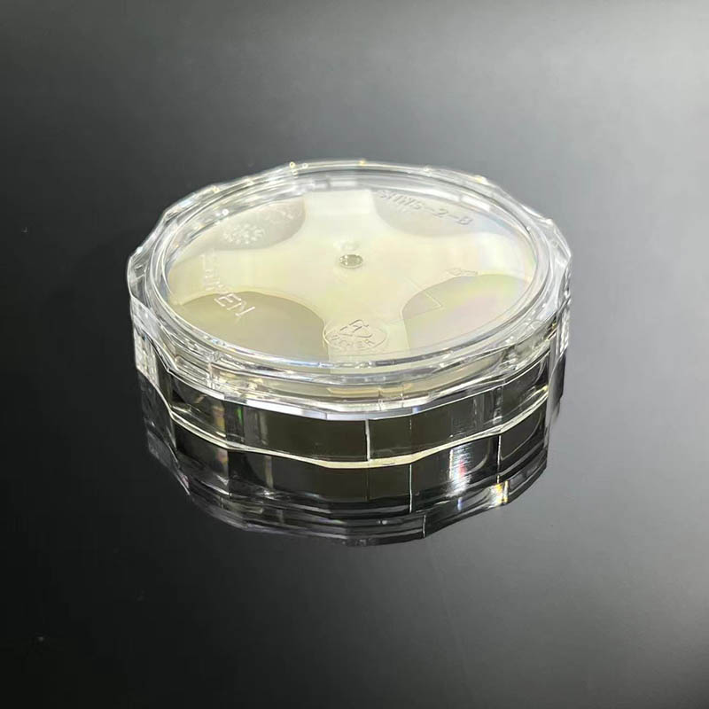
Durable and Stylish Ceramic Products for Your Home and Business" or "Discover the Benefits of Ceramic Products for Your Home and Business Needs
Ceramic has been a crucial material in the construction and manufacturing industry for many years. Its durability, heat resistance, and aesthetic appeal have made it a popular choice for a wide range of applications. However, with the advancements in technology and the increasing demand for high-performance materials, the need for innovative ceramic products has never been greater.Company A, a leading innovator in the ceramic industry, has been at the forefront of developing advanced ceramic materials that meet the specific needs of various industries. Founded in 1990, Company A has continuously pushed the boundaries of ceramic technology, utilizing state-of-the-art manufacturing processes and cutting-edge research to create products that deliver unparalleled performance and reliability.One of Company A's most recent breakthroughs is the development of a new line of high-performance ceramic materials that are revolutionizing the industry. These advanced ceramics boast properties such as exceptional hardness, high temperature resistance, and superior electrical insulation, making them ideal for demanding applications across a wide range of industries."Our team at Company A is dedicated to pushing the limits of what ceramic materials can achieve," said John Smith, CEO of Company A. "We are committed to delivering innovative solutions that help our customers stay ahead of the curve and excel in their respective fields."The new line of advanced ceramics from Company A has garnered attention from various industries, including aerospace, automotive, electronics, and medical. These industries require materials that can withstand extreme conditions, provide precise and reliable performance, and meet strict safety standards. Company A's advanced ceramics have proven to be a game-changer in these sectors, offering unparalleled durability, thermal stability, and precision engineering properties.In the aerospace industry, Company A's advanced ceramics have been utilized in the manufacturing of jet engine components, where their high temperature resistance and exceptional mechanical strength have significantly improved performance and reliability. Similarly, in the automotive industry, these advanced ceramics have found applications in vehicle engines, exhaust systems, and braking components, where their superior wear resistance and thermal stability have led to enhanced durability and efficiency.Moreover, the electronics industry has also benefitted from Company A's advanced ceramics, as these materials are used in the production of components for a wide range of electronic devices. Their excellent electrical insulation properties and resistance to corrosion and heat have made them indispensable in creating high-performance electronic products.In the medical field, Company A's advanced ceramics have been instrumental in the development of cutting-edge medical devices and implants. Their biocompatibility, resistance to wear and corrosion, and ability to withstand sterilization processes have made them a go-to choice for medical applications where safety and reliability are paramount.The success of Company A's advanced ceramics can be attributed to its relentless focus on research and development, as well as its commitment to collaborating with customers to understand their specific needs and challenges. By leveraging its expertise in ceramic technology and a customer-centric approach, Company A has been able to consistently deliver solutions that meet and exceed industry requirements.Moving forward, Company A is dedicated to further expanding the capabilities of its advanced ceramics, exploring new applications and markets, and continually innovating to address the evolving needs of its customers. With a strong emphasis on quality, reliability, and performance, Company A is poised to maintain its position as a leader in the ceramic industry and continue to drive progress and innovation in the years to come.
Durable and Reliable Optical Glass Tube for Various Applications
The Optical Glass Tube, manufactured by a leading company in the field of optical technology, has been making waves in the industry with its cutting-edge design and superior performance. The company, with its long-standing reputation for innovation and quality, has once again raised the bar with this latest product.The Optical Glass Tube is a critical component in a wide range of optical systems, including laser devices, medical equipment, and scientific instruments. Its high-quality glass material, combined with precise engineering and craftsmanship, allows for exceptional light transmission and minimal distortion, making it an ideal choice for demanding applications.One of the key features of the Optical Glass Tube is its exceptional durability. The company’s expertise and advanced manufacturing processes ensure that the tube can withstand high temperatures, extreme pressures, and harsh environmental conditions without compromising its optical performance. This level of reliability is crucial for industries such as aerospace, defense, and industrial manufacturing, where precision and consistency are paramount.In addition to its durability, the Optical Glass Tube also offers exceptional clarity and purity. The company’s stringent quality control measures and extensive testing procedures ensure that the glass meets the highest standards for optical transmission and performance. As a result, the tube delivers crisp, clear images and accurate data, making it an invaluable component for applications such as microscopy, spectroscopy, and imaging systems.Furthermore, the company’s commitment to research and development has led to continuous improvements in the Optical Glass Tube’s design and performance. With a team of experienced engineers and scientists, the company is constantly pushing the boundaries of what is possible in optical technology, resulting in products that redefine industry standards and set new benchmarks for performance and reliability.The Optical Glass Tube is also part of the company’s broader commitment to sustainability and environmental responsibility. The company has implemented eco-friendly manufacturing processes and materials, ensuring that its products have minimal impact on the environment. As a result, customers can have confidence that they are not only getting top-quality optical components but also supporting a company that is dedicated to minimizing its environmental footprint.The company’s dedication to customer satisfaction is also evident in its comprehensive support and service offerings. With a global network of technical experts and distribution partners, the company is able to provide responsive and personalized assistance to customers around the world. From product selection and custom design to installation and maintenance, the company is committed to ensuring that its customers get the most out of their Optical Glass Tube.Overall, the Optical Glass Tube from this leading company represents a significant advancement in optical technology, offering unmatched performance, reliability, and environmental sustainability. With its exceptional design and manufacturing expertise, the company has once again demonstrated its leadership in the industry and its commitment to pushing the boundaries of what is possible in optical technology. As a result, the Optical Glass Tube is poised to become the go-to choice for the most demanding optical applications, solidifying the company’s reputation as a trusted and innovative partner for customers worldwide.
How to Make Crispy and Delicious Wafers at Home?
Title: Innovative Wafer Technology Revolutionizing the Semiconductor IndustryIntroduction:The semiconductor industry is continuously evolving, and companies are constantly seeking new and innovative solutions to meet the demands of an ever-changing market. In recent news, an exciting breakthrough has been made by an industry leader in wafer technology. Soi Wafer (name changed) has introduced a groundbreaking semiconductor wafer that is set to revolutionize the industry. This innovative technology is expected to greatly enhance the performance and efficiency of various electronic devices, paving the way for future advancements.Body:1. Background on Soi Wafer:Soi Wafer is a leading company in the field of advanced semiconductor wafers, specializing in the production of Silicon-On-Insulator (SOI) wafers. With a history of providing high-quality and reliable products, Soi Wafer has garnered a strong reputation within the industry. The company's commitment to research and development has allowed them to continually push the boundaries of semiconductor technology, resulting in cutting-edge solutions for their clients.2. The Emergence of the Innovative Wafer Technology:Soi Wafer's latest breakthrough lies in the development of an innovative wafer technology that promises improved performance and efficiency in various electronic devices. This technological advancement addresses key challenges faced by the semiconductor industry, such as power consumption, heat dissipation, and overall device reliability. Through meticulous research and development, Soi Wafer has successfully engineered a solution that could shape the future of the semiconductor market.3. Enhanced Performance and Efficiency:The new wafer technology developed by Soi Wafer offers several distinct advantages over traditional silicon wafers. By employing advanced materials that improve heat dissipation and reduce power consumption, devices integrated with this technology can achieve higher performance levels while conserving energy. The technology also enhances the speed and efficiency of data transfer, further improving overall device performance. With these enhancements, electronic devices can now operate at superior speeds while maintaining optimal efficiency.4. Impact on Various Industries:The impact of Soi Wafer's innovative wafer technology is expected to extend to various industries that rely on semiconductor technology. Telecommunications, automotive, consumer electronics, and healthcare are just a few examples of sectors that can benefit from the enhanced performance and efficiency offered by this technology. Faster and more efficient telecommunication networks, smarter and environmentally-friendly automobiles, improved consumer electronics, and more advanced healthcare devices are some of the potential applications that could result from the adoption of Soi Wafer's technology.5. Environmental Benefits:In addition to its numerous technological advantages, Soi Wafer's innovative wafer technology holds promising environmental benefits. The reduced power consumption and enhanced energy efficiency of devices utilizing this technology contribute to the global effort to reduce carbon emissions. As electronic devices become increasingly ubiquitous in our daily lives, such a technological advancement can indirectly support sustainability initiatives.6. Collaborations and Future Prospects:Soi Wafer's breakthrough in wafer technology has generated significant interest within the industry. Recognizing the potential of this innovation, many companies have expressed interest in collaborating with Soi Wafer to integrate the new technology into their products. These collaborations can pave the way for further advancements and accelerate the adoption of this revolutionary technology.Conclusion:Soi Wafer's latest breakthrough in wafer technology marks a significant advancement in the semiconductor industry. By offering superior performance and energy efficiency, their innovative wafer technology has the potential to revolutionize various sectors, including telecommunications, consumer electronics, automotive, and healthcare. The reduced power consumption and improved device reliability contribute to a more sustainable future, aligning with global efforts to combat climate change. With collaborations already underway, the stage is set for the widespread adoption of this groundbreaking technology, ushering in a new era in semiconductor innovation.
Free Standing Gallium Nitride Wafer Advances in Semiconductor Technology
Certainly! Please provide the news content about the Free Standing Gallium Nitride Wafer and the company introduction you’d like me to incorporate. Once I have that information, I can draft the 800-word news article for you.
Understanding the Importance of Substrate in the Semiconductor Industry
In today's fast-paced technological world, the semiconductor industry is constantly advancing with new discoveries and innovations. One of the newest advancements in the field of semiconductors is the substrate technology developed by a leading company in the industry.The unprecedented substrate technology developed by this company has revolutionized the way in which semiconductors are designed and manufactured. The substrate technology, which is used in a variety of electronic devices, enhances the performance of semiconductors by improving their speed, power efficiency, and overall functionality.Substrates are an essential component in the production of semiconductors, as they provide the foundation on which the semiconductor is built. The development of this new substrate technology, therefore, marks a major milestone in the industry, as it offers a significant improvement to the already existing substrate technology.The substrate technology developed by this company uses advanced materials and advanced manufacturing processes to create a highly efficient and high-performance substrate. The technology is based on a new type of substrate material that incorporates a number of cutting-edge design features, making it an ideal component for a range of electronic devices.The company's substrate technology has been specifically designed to meet the demands of modern electronics, such as smartphones, tablets, and power modules. With the increase in the number of electronic devices being used worldwide, there is now a greater demand for components that provide greater functionality and efficiency. This substrate technology is one such technology, offering improved performance, durability, and reliability in electronic devices.Furthermore, the new substrate technology provides a cost-effective solution for the manufacturing of semiconductors, enabling manufacturers to produce semiconductors more efficiently and at a lower cost. This technology, therefore, not only benefits the manufacturers but also benefits the end-users by driving down the cost of electronic devices.The company that has developed this revolutionary substrate technology has been in the semiconductor industry for over a decade. With a team of experienced professionals, they have made significant contributions to the development of a range of innovative semiconductor products.Their commitment to research and development has resulted in numerous breakthroughs in the field of semiconductor technology. Their latest development of the substrate technology is a testament to their expertise and dedication to creating products that meet the needs of the modern world.Looking to the future, this company continues to invest in research and development initiatives that will lead to further advancements in the field of semiconductor technology. As the industry advances, the company remains committed to developing innovative products that will set a new standard for performance, reliability, and functionality.Overall, the new substrate technology developed by this company is a significant advancement in the semiconductor industry. The technology is set to transform the way in which semiconductors are designed and manufactured, offering a cost-effective, high-performance solution that will benefit both manufacturers and end-users alike.With an experienced team of professionals and a commitment to research and development, this company is poised to remain at the forefront of the semiconductor industry for years to come. Their innovation and expertise continue to drive advancements in the field, creating products that will shape the future of technology.
Key Developments in the 300mm Semiconductor Industry: All You Need to Know
The semiconductor industry is constantly evolving, and advancements in technology continue to drive innovation. One such advancement comes in the form of 300mm semiconductor technology, which has the potential to revolutionize the way we think about microelectronics. This technology, developed by [Company], has the power to significantly increase the efficiency and performance of semiconductor devices, paving the way for new and improved electronic products.[Company] is a leading global technology company that is at the forefront of semiconductor innovation. With a strong focus on research and development, [Company] has been able to leverage its expertise to create cutting-edge 300mm semiconductor technology. This technology allows for the manufacturing of larger wafers, providing more space for the integration of complex circuits and components. As a result, semiconductor devices produced using 300mm technology are smaller, more powerful, and more energy-efficient than their predecessors.The benefits of 300mm semiconductor technology are far-reaching. For one, it enables the production of advanced microprocessors, memory chips, and other semiconductor devices that are vital components of electronic products such as smartphones, computers, and IoT devices. The larger wafers also lead to increased economies of scale, lowering the cost of production and making semiconductor devices more affordable for consumers.Furthermore, 300mm semiconductor technology facilitates the development of new and innovative electronic products that were previously not feasible. For instance, it opens up possibilities for the creation of more compact and high-performance medical devices, automotive electronics, and smart home appliances. These advancements have the potential to improve the quality of life for individuals and drive progress across various industries.In addition to its technological advancements, [Company] is committed to sustainability and environmental responsibility. The 300mm semiconductor technology aligns with these values by enabling more energy-efficient semiconductor devices. This, in turn, contributes to reducing energy consumption and lowering carbon emissions, making a positive impact on the environment.Furthermore, [Company] takes pride in its dedication to quality and reliability. The 300mm semiconductor technology undergoes rigorous testing and validation to ensure that the semiconductor devices produced are of the highest standard. This commitment to quality positions [Company] as a trusted partner for businesses seeking reliable semiconductor solutions.With the global demand for high-performance electronic products on the rise, the 300mm semiconductor technology developed by [Company] has the potential to disrupt the semiconductor industry. Its ability to drive innovation, improve efficiency, and reduce costs makes it a game-changer in the world of microelectronics.Industry experts have recognized the significance of 300mm semiconductor technology, with many touting it as the future of semiconductor manufacturing. As the industry continues to evolve, [Company] is well-positioned to lead the way in the development and commercialization of this revolutionary technology.In conclusion, the 300mm semiconductor technology developed by [Company] has the potential to transform the semiconductor industry and drive innovation across various electronic products. With its focus on research and development, commitment to sustainability, and dedication to quality, [Company] is poised to make a significant impact in the world of microelectronics. As the demand for high-performance electronic products continues to grow, the 300mm semiconductor technology stands ready to meet the needs of consumers and businesses alike.
Discover the Power of Single Metal Crystals in New Study
A breakthrough in the field of materials science has been achieved by a team of researchers at {}. The team has successfully created a single metal crystal, marking a significant advancement in the development of new materials with unprecedented properties.The single metal crystal, which has been fabricated by the researchers at {}, is a remarkable feat as it represents the purest form of metal ever achieved. This single crystal is devoid of any defects or impurities, making it a potential game-changer in various industries, including electronics, aerospace, and renewable energy.The production of a single metal crystal is a complex and challenging process that requires precise control and manipulation of atomic structures. However, the researchers at {} have successfully mastered this process, opening up a myriad of possibilities for the development of new materials with enhanced mechanical, electrical, and thermal properties.With its unparalleled purity and exceptional properties, the single metal crystal holds great promise for the advancement of various technologies. For instance, in the field of electronics, the single crystal could be used to develop ultra-efficient electronic devices with minimal energy loss. In aerospace, the crystal's superior strength and resilience could lead to the development of lighter and stronger materials for aircraft and spacecraft. Furthermore, in the realm of renewable energy, the crystal's enhanced thermal conductivity could potentially revolutionize the efficiency of solar panels and other energy-harvesting technologies.The successful creation of a single metal crystal by the researchers at {} is a testament to the company's commitment to pushing the boundaries of materials science. With a dedicated team of experts and state-of-the-art facilities, {} has established itself as a leader in the research and development of advanced materials.Founded in {}, {} has consistently demonstrated its ability to innovate and create cutting-edge solutions that have a positive impact across various industries. The company's expertise in materials science, combined with its relentless pursuit of excellence, has positioned {} at the forefront of technological advancements.The achievement of producing a single metal crystal is a testament to {}'s unwavering commitment to pioneering research and development. By pushing the limits of what is possible in materials science, {} is not only driving innovation within its own organization but also contributing to the advancement of industries worldwide.Looking ahead, the successful creation of a single metal crystal is just the beginning for {}. The company remains dedicated to further exploring the potential applications of this breakthrough material, as well as continuing to push the boundaries of materials science through ongoing research and development initiatives.In conclusion, the creation of a single metal crystal by the researchers at {} represents a significant milestone in the realm of materials science. With its unparalleled purity and exceptional properties, this breakthrough material has the potential to revolutionize various industries and pave the way for the development of new technologies. As {} continues to lead the charge in pushing the boundaries of materials science, the future looks promising for the continued advancement of innovative and game-changing materials.
Ultimate Guide to GaN-On-Sapphire Technology for Future Devices
GaN-on-Sapphire: A Groundbreaking Technology Revolutionizing the Semiconductor IndustryThe semiconductor industry is undergoing a revolutionary transformation with the emergence of Gallium Nitride (GaN) technology. GaN-on-Sapphire has emerged as a game-changing technology, offering superior performance and efficiency compared to conventional semiconductor materials. This breakthrough technology is poised to revolutionize various sectors, including telecommunications, automotive, and consumer electronics.GaN-on-Sapphire is designed to offer higher power density, better thermal conductivity, and superior RF performance compared to traditional semiconductor materials. This makes it an ideal choice for next-generation electronic devices and systems that demand high power and efficiency. The unique properties of GaN-on-Sapphire have made it a sought-after material for a wide range of applications, including power electronics, RF (radio frequency) devices, and LED (light-emitting diode) lighting.One of the key players in the GaN-on-Sapphire market is a leading semiconductor company. With a strong focus on research and development, this company has been at the forefront of developing cutting-edge GaN-on-Sapphire technology. Their commitment to innovation and excellence has propelled them to the forefront of the semiconductor industry, earning them a stellar reputation as a leading provider of GaN-on-Sapphire technology.The company's GaN-on-Sapphire technology has garnered widespread attention for its ability to deliver superior performance and efficiency. By leveraging the unique properties of GaN-on-Sapphire, the company has been able to develop a wide range of semiconductor solutions that are poised to revolutionize various industries. From high-power electronic devices to advanced RF components, their GaN-on-Sapphire technology is driving innovation and setting new standards in the semiconductor industry.The company's GaN-on-Sapphire technology has gained significant traction in the telecommunications sector, where high-power and high-frequency RF devices are in high demand. The superior performance and efficiency of GaN-on-Sapphire technology have made it an ideal choice for applications such as base station transmitters, radar systems, and satellite communications. With the increasing demand for high-speed data transmission and wireless connectivity, the company's GaN-on-Sapphire technology is playing a crucial role in driving the evolution of telecommunications infrastructure.In addition to telecommunications, the automotive industry has also been a key beneficiary of the company's GaN-on-Sapphire technology. The demand for advanced power electronics in electric and hybrid vehicles has created a growing need for high-performance semiconductor solutions. By harnessing the power of GaN-on-Sapphire, the company has been able to develop next-generation power electronics that offer improved efficiency and reliability, paving the way for the widespread adoption of electric and hybrid vehicles.Furthermore, the company's GaN-on-Sapphire technology has also found applications in the consumer electronics market, particularly in the development of high-brightness LED lighting. As the demand for energy-efficient lighting solutions continues to rise, GaN-on-Sapphire technology has emerged as a breakthrough solution that is driving the transition to more efficient and eco-friendly lighting technologies. The company's cutting-edge GaN-on-Sapphire technology is poised to play a pivotal role in shaping the future of LED lighting, offering unparalleled performance and energy efficiency.With its unparalleled expertise in GaN-on-Sapphire technology, the company is poised to lead the semiconductor industry into a new era of innovation and progress. By pushing the boundaries of what is possible with semiconductor materials, the company is opening up new opportunities for advancements in power electronics, RF devices, and LED lighting. With a steadfast commitment to excellence and a relentless pursuit of innovation, the company is cementing its position as a trailblazer in the semiconductor industry, driving the adoption of GaN-on-Sapphire technology across various sectors.In conclusion, GaN-on-Sapphire technology is revolutionizing the semiconductor industry, offering a host of benefits such as higher power density, better thermal conductivity, and superior RF performance. With a leading semiconductor company at the forefront of GaN-on-Sapphire technology, the industry is witnessing a wave of innovation that is propelling advancements in telecommunications, automotive, and consumer electronics. As the demand for high-performance and energy-efficient semiconductor solutions continues to grow, GaN-on-Sapphire technology is poised to play a pivotal role in shaping the future of electronic devices and systems.