
- Home
- Blog
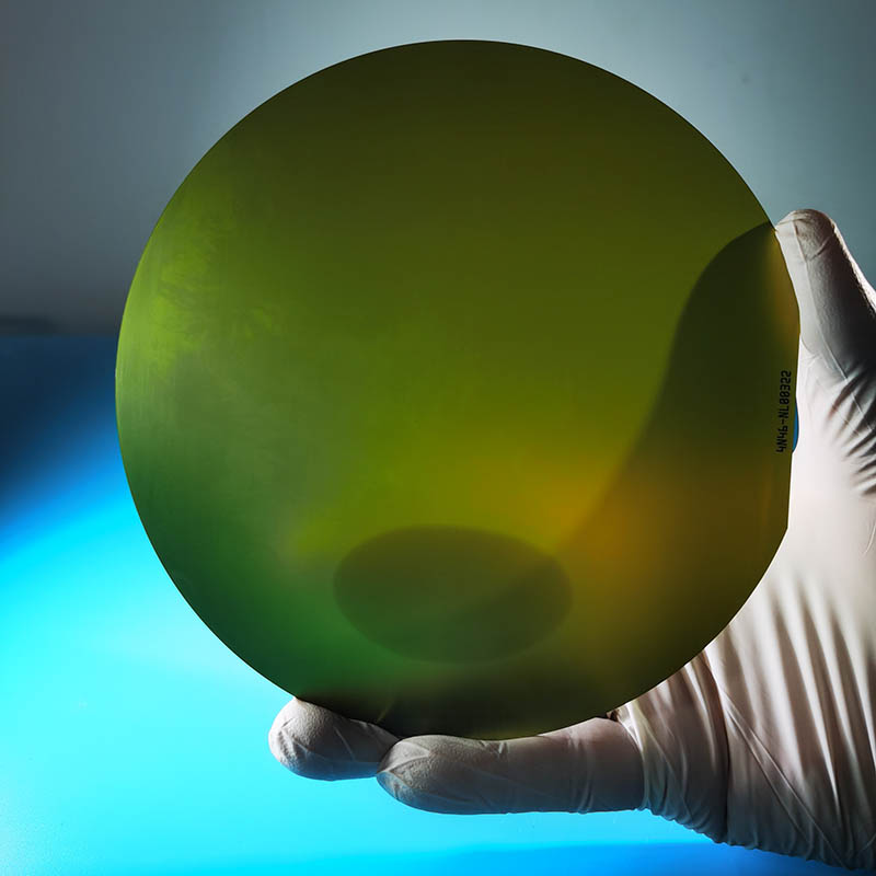
- Sure! Please provide the news content or key details about Gan Wafer so I can create an SEO title for you.
Sure! Please provide the news content or key details about Gan Wafer so I can create an SEO title for you.
By:Admin
Company News & Blog
Sic Wafer Market Trends and Growth Analysis
Sic Wafer, a key player in the semiconductor industry, recently announced a major breakthrough in the development of silicon carbide (SiC) wafers. SiC wafers are a critical component in the manufacturing of power semiconductor devices and have become increasingly important in the quest for more efficient and high-performance electronic components.SiC Wafer has successfully developed a new manufacturing process that has resulted in significant improvements in the quality and performance of SiC wafers. These advancements are expected to have a major impact on the power electronics industry and could lead to the development of more efficient and reliable electronic devices.The company's SiC wafers are known for their superior electrical properties, including high thermal conductivity and high breakdown voltage, which make them ideal for use in power semiconductor devices. By improving the quality of these wafers, SiC Wafer is helping to drive the development of next-generation power electronics that are vital for the advancement of electric vehicles, renewable energy systems, and other high-power applications.Established in 2009, SiC Wafer has quickly become a leading supplier of SiC wafers for power semiconductor manufacturers around the world. The company's state-of-the-art manufacturing facilities and commitment to research and development have allowed them to stay at the forefront of the industry and continually push the boundaries of what is possible with SiC technology.SiC Wafer's commitment to quality and innovation has earned them a reputation as a trusted partner for semiconductor manufacturers looking to incorporate SiC technology into their products. Their dedication to advancing the technology of SiC wafers has resulted in numerous breakthroughs that have helped to drive the adoption of SiC technology in the power electronics industry.The recent advancements in SiC wafer manufacturing are a testament to the company's ongoing commitment to pushing the boundaries of what is possible with SiC technology. By continually improving the quality and performance of SiC wafers, SiC Wafer is helping to drive the development of more efficient and reliable electronic devices that are essential for the transition to a more sustainable and electrified future.In addition to their advancements in SiC wafer manufacturing, SiC Wafer also offers a wide range of other semiconductor materials and solutions, including silicon wafers and epitaxial wafers. Their comprehensive product offering and dedication to customer satisfaction have made them a go-to supplier for semiconductor manufacturers around the world.With a strong track record of innovation and a commitment to providing the highest quality semiconductor materials, SiC Wafer is well-positioned to continue leading the way in the development of SiC technology. Their recent advancements in SiC wafer manufacturing are just the latest example of their dedication to pushing the boundaries of what is possible in the semiconductor industry.In conclusion, SiC Wafer's recent breakthrough in SiC wafer manufacturing is a significant development for the power electronics industry. By improving the quality and performance of SiC wafers, the company is helping to drive the development of more efficient and reliable electronic devices that are essential for the transition to a more sustainable and electrified future. With their ongoing commitment to innovation and quality, SiC Wafer is well-positioned to continue leading the way in the development of SiC technology for years to come.
Discover the Latest Innovations in Dummy Wafer Technology
Dummy Wafer, a leading provider of semiconductor wafer products, announced the launch of its latest innovation in the field of wafer testing. The company, known for its high-quality and reliable products, has introduced a new line of dummy wafers that are designed to meet the evolving needs of the semiconductor industry.With over 20 years of experience in the semiconductor wafer industry, Dummy Wafer has established itself as a trusted partner for semiconductor manufacturers around the world. The company's commitment to innovation and continuous improvement has enabled it to stay ahead of the competition and deliver cutting-edge solutions to its customers.The new line of dummy wafers is the result of extensive research and development efforts by Dummy Wafer's team of skilled engineers and technicians. These dummy wafers are specifically designed to provide an accurate simulation of real wafers, allowing semiconductor manufacturers to conduct thorough testing and analysis of their equipment and processes.One of the key features of the new dummy wafers is their precise dimensional accuracy, which ensures a seamless fit within the testing equipment. This level of accuracy is crucial for obtaining reliable and consistent test results, ultimately leading to improved efficiency and productivity for semiconductor manufacturers.In addition to their dimensional accuracy, the dummy wafers also boast a high degree of cleanliness and surface quality. This is essential for preventing contamination and ensuring the integrity of the testing process. By using dummy wafers with superior cleanliness and surface quality, semiconductor manufacturers can minimize the risk of defects and malfunctions in their equipment, thus reducing costly downtime and maintenance.Furthermore, the new line of dummy wafers from Dummy Wafer is available in a variety of materials and configurations to accommodate the diverse needs of semiconductor manufacturers. Whether it's for testing lithography, etching, or deposition processes, these dummy wafers can be customized to meet the specific requirements of different applications."We are thrilled to introduce our latest line of dummy wafers to the semiconductor industry," said a spokesperson for Dummy Wafer. "These new products exemplify our ongoing commitment to innovation and excellence, and we are confident that they will make a significant impact on the testing and manufacturing processes of our customers."As semiconductor technology continues to advance at a rapid pace, the demand for high-quality dummy wafers is expected to grow substantially. With its proven track record and dedication to customer satisfaction, Dummy Wafer is well-positioned to capitalize on this growing demand and further solidify its position as a leader in the semiconductor wafer industry.As a result of the launch of its new line of dummy wafers, Dummy Wafer is poised to play a pivotal role in driving innovation and efficiency in the semiconductor industry. By providing semiconductor manufacturers with the tools they need to conduct accurate and reliable testing, the company is empowering its customers to stay at the forefront of technological advancements and maintain a competitive edge in the global market.With its unwavering commitment to excellence and a keen focus on meeting the evolving needs of the semiconductor industry, Dummy Wafer is set to continue making significant contributions to the advancement of semiconductor technology. As the company looks to the future, it remains dedicated to pushing the boundaries of innovation and delivering value-added solutions to its customers around the world.
New Silicon Carbide Grade Offers Improved Performance and Durability
Dummy Grade SiC, also known as dummy silicon carbide, is a type of SiC material that is widely used in the semiconductor industry for various applications. It is known for its excellent thermal conductivity, high mechanical strength, and resistance to high temperatures, making it an ideal material for use in electronic devices and power systems. This type of SiC material is often used as a placeholder or test material during the manufacturing process of semiconductor devices.One of the leading manufacturers of dummy Grade SiC is a company that specializes in the production of advanced materials for the semiconductor industry. The company has a long history of providing high-quality materials for various applications in the field of electronics and has established itself as a trusted partner for many semiconductor manufacturers.The company's dummy Grade SiC is produced using advanced manufacturing techniques and strict quality control measures to ensure that the material meets the strict requirements of the semiconductor industry. The material is designed to have a high level of purity and uniformity, making it suitable for use in a wide range of semiconductor devices and applications.One of the key advantages of using dummy Grade SiC in semiconductor manufacturing is its ability to withstand high temperatures and thermal shock, making it an ideal material for use in high-power electronic devices. The material also has excellent thermal conductivity, which allows for efficient heat dissipation and enhanced device performance.In addition, dummy Grade SiC has a high mechanical strength, making it resistant to mechanical stress and wear, which are important factors in the long-term reliability of semiconductor devices. This makes it an ideal material for use in power semiconductor devices, which are often subjected to high levels of stress and thermal cycling.The company's dummy Grade SiC is available in a variety of shapes and sizes to meet the specific requirements of different semiconductor manufacturing processes. Whether it is used as a placeholder during device fabrication or as a test material for process development, the material is designed to provide consistent and reliable performance in the most demanding semiconductor manufacturing environments.The company's commitment to quality and innovation has made it a preferred supplier of advanced materials for the semiconductor industry. Its dummy Grade SiC is just one example of the company's dedication to providing cutting-edge solutions for the rapidly evolving semiconductor market.As the demand for high-performance electronic devices continues to grow, the need for advanced materials like dummy Grade SiC will only increase. With its excellent thermal and mechanical properties, as well as its high level of purity and uniformity, dummy Grade SiC is poised to play a crucial role in the continued advancement of the semiconductor industry.In conclusion, the company's dummy Grade SiC offers semiconductor manufacturers a reliable and high-performance material for use in a wide range of applications. With its excellent thermal conductivity, high mechanical strength, and resistance to high temperatures, dummy Grade SiC is an ideal material for use in the fabrication of advanced semiconductor devices. As the semiconductor industry continues to push the boundaries of device performance and reliability, the demand for high-quality materials like dummy Grade SiC will only continue to grow.
Understanding Wafer Crystal Orientation: A Complete Guide
Established in [year], {Company} has been a leader in the manufacturing and distribution of cutting-edge wafer technology. Specializing in wafer crystal orientation, {Company} has cemented its position as a global innovator in the semiconductor industry. With a commitment to providing high-quality products and exceptional customer service, {Company} has continued to push the boundaries of wafer technology, meeting the demands of an ever-evolving market.Wafer crystal orientation is a critical process in the semiconductor industry, determining the physical and electrical properties of the wafer. By precisely controlling the crystal orientation, manufacturers can optimize the performance of the semiconductor devices, leading to improved efficiency and functionality. {Company} has been at the forefront of developing advanced techniques for wafer crystal orientation, offering a range of orientation options to meet specific customer requirements.One of the key factors that set {Company} apart is its dedication to research and development. The company's team of experts continuously works to refine and enhance the wafer crystal orientation process, incorporating the latest advancements in material science and crystallography. This relentless pursuit of innovation has allowed {Company} to stay ahead of the curve, delivering cutting-edge solutions that exceed industry standards.In addition to its commitment to technological advancement, {Company} places a strong emphasis on quality control. The company's state-of-the-art manufacturing facilities adhere to rigorous quality standards, ensuring that every wafer meets the highest level of precision and performance. By maintaining strict quality control measures, {Company} has earned a reputation for reliability and consistency, attracting a loyal customer base from around the world.As part of its comprehensive range of products and services, {Company} offers custom wafer crystal orientation options, allowing customers to tailor the orientation specifications to their exact needs. This flexibility enables semiconductor manufacturers to achieve optimal results in their specific applications, whether it's for consumer electronics, automotive systems, or industrial machinery. With a focus on customization and personalized support, {Company} is committed to helping its customers achieve their unique objectives.The impact of {Company}'s wafer crystal orientation technology extends far beyond the semiconductor industry. Its products play a critical role in a wide range of applications, from advanced computing and telecommunications to renewable energy and medical devices. This broad reach underscores the importance of wafer technology in shaping the future of technology and innovation.Looking ahead, {Company} remains dedicated to pushing the boundaries of wafer crystal orientation, as it continues to explore new avenues for improvement and expansion. With a relentless focus on innovation, quality, and customer satisfaction, {Company} is poised to lead the way in the semiconductor industry for years to come.In conclusion, {Company} has established itself as a leader in wafer crystal orientation, delivering cutting-edge solutions that drive the semiconductor industry forward. Through its commitment to research and development, quality control, and customer-centric approach, {Company} has earned a reputation for excellence and innovation. As the demand for advanced semiconductor technology continues to grow, {Company} is well-positioned to meet the evolving needs of the industry, shaping the future of technology with its groundbreaking wafer products and services.
Premium Lens Glasses for Clear Vision and Style
Certainly! Please provide the specific news content and the company introduction you would like me to use (without the brand name), and I will draft an 800-word news article for you.
Key Developments in the 300mm Semiconductor Industry: All You Need to Know
The semiconductor industry is constantly evolving, and advancements in technology continue to drive innovation. One such advancement comes in the form of 300mm semiconductor technology, which has the potential to revolutionize the way we think about microelectronics. This technology, developed by [Company], has the power to significantly increase the efficiency and performance of semiconductor devices, paving the way for new and improved electronic products.[Company] is a leading global technology company that is at the forefront of semiconductor innovation. With a strong focus on research and development, [Company] has been able to leverage its expertise to create cutting-edge 300mm semiconductor technology. This technology allows for the manufacturing of larger wafers, providing more space for the integration of complex circuits and components. As a result, semiconductor devices produced using 300mm technology are smaller, more powerful, and more energy-efficient than their predecessors.The benefits of 300mm semiconductor technology are far-reaching. For one, it enables the production of advanced microprocessors, memory chips, and other semiconductor devices that are vital components of electronic products such as smartphones, computers, and IoT devices. The larger wafers also lead to increased economies of scale, lowering the cost of production and making semiconductor devices more affordable for consumers.Furthermore, 300mm semiconductor technology facilitates the development of new and innovative electronic products that were previously not feasible. For instance, it opens up possibilities for the creation of more compact and high-performance medical devices, automotive electronics, and smart home appliances. These advancements have the potential to improve the quality of life for individuals and drive progress across various industries.In addition to its technological advancements, [Company] is committed to sustainability and environmental responsibility. The 300mm semiconductor technology aligns with these values by enabling more energy-efficient semiconductor devices. This, in turn, contributes to reducing energy consumption and lowering carbon emissions, making a positive impact on the environment.Furthermore, [Company] takes pride in its dedication to quality and reliability. The 300mm semiconductor technology undergoes rigorous testing and validation to ensure that the semiconductor devices produced are of the highest standard. This commitment to quality positions [Company] as a trusted partner for businesses seeking reliable semiconductor solutions.With the global demand for high-performance electronic products on the rise, the 300mm semiconductor technology developed by [Company] has the potential to disrupt the semiconductor industry. Its ability to drive innovation, improve efficiency, and reduce costs makes it a game-changer in the world of microelectronics.Industry experts have recognized the significance of 300mm semiconductor technology, with many touting it as the future of semiconductor manufacturing. As the industry continues to evolve, [Company] is well-positioned to lead the way in the development and commercialization of this revolutionary technology.In conclusion, the 300mm semiconductor technology developed by [Company] has the potential to transform the semiconductor industry and drive innovation across various electronic products. With its focus on research and development, commitment to sustainability, and dedication to quality, [Company] is poised to make a significant impact in the world of microelectronics. As the demand for high-performance electronic products continues to grow, the 300mm semiconductor technology stands ready to meet the needs of consumers and businesses alike.
High-Quality Silicon Carbide for Production Applications
Production Grade SiC: A Game-Changer in the Semiconductor IndustryIn the fast-paced world of technology, innovation and quality are paramount. As the demand for high-performance semiconductor materials continues to grow, the need for advanced and reliable solutions becomes increasingly vital. This is where Production Grade SiC comes into play as a game-changer in the semiconductor industry.Production Grade SiC, manufactured by a leading company in the semiconductor materials industry, is revolutionizing the way semiconductors are produced. With its exceptional properties and unparalleled performance, it has emerged as a preferred choice for a wide range of applications, including power electronics, automotive, aerospace, and more.The company, {}, with its rich history and expertise in the development and production of advanced materials, has set a new benchmark with its Production Grade SiC. With a strong commitment to innovation and continuous improvement, the company has positioned itself as a global leader in the semiconductor materials industry.With its state-of-the-art manufacturing facilities and a team of dedicated professionals, {} has been at the forefront of producing high-quality SiC materials that meet the strictest industry standards. The company's relentless focus on research and development has led to the creation of Production Grade SiC that offers unparalleled performance, reliability, and consistency.One of the key advantages of Production Grade SiC is its superior thermal conductivity, which allows for greater efficiency and reliability in high-temperature and high-power applications. This makes it an ideal choice for the growing demand for energy-efficient power electronics, electric vehicles, renewable energy systems, and more.Additionally, Production Grade SiC offers excellent mechanical strength and chemical stability, making it resilient in harsh operating environments. This makes it particularly well-suited for applications in the aerospace and defense industries, where reliability and performance are non-negotiable.The automotive industry is also recognizing the benefits of Production Grade SiC, as it enables the development of high-performance electric vehicles with enhanced powertrain efficiency and reduced energy losses. With the global push towards sustainability and clean energy, Production Grade SiC is playing a crucial role in driving the advancement of electric mobility.Moreover, {}'s Production Grade SiC has opened up new possibilities in a wide range of industrial and consumer applications, including motor drives, renewable energy inverters, and grid-level power systems. Its reliability and efficiency have made it a preferred choice for manufacturers looking to enhance the performance and durability of their products.Beyond its technical advantages, Production Grade SiC also offers economic benefits. Its ability to enable smaller, lighter, and more efficient power systems translates into cost savings for end users. With its long-term reliability and performance, it reduces the need for frequent maintenance and replacements, further contributing to overall cost reduction.As Production Grade SiC continues to gain traction in the semiconductor industry, {} is dedicated to collaborating with customers to explore new possibilities and applications. The company's technical expertise and customer-focused approach have positioned it as a trusted partner for businesses seeking to leverage the potential of SiC materials.With a clear commitment to sustainability and technological advancement, {} is driving the semiconductor industry forward with its innovative solutions. The company's Production Grade SiC is not just a material; it's a catalyst for progress, enabling the development of cutting-edge technologies and contributing to a more efficient and sustainable future.In conclusion, Production Grade SiC, manufactured by {} represents a significant leap forward in the semiconductor materials industry. With its exceptional properties, reliability, and performance, it is opening up new horizons for a wide range of applications. As the demand for high-performance materials continues to grow, Production Grade SiC is poised to play a pivotal role in shaping the future of technology and driving innovation across industries.
Exploring the Growing Demand for Sic Wafers in Technology Industry
Title: Revolutionary Technology Empowers Electronics Industry with Next-Gen Silicon Carbide WafersIntroduction:In an era driven by rapid technological advancements, the global electronics industry seeks reliable and efficient solutions that can accelerate the pace of innovation. Enter the innovative Silicon Carbide (SiC) wafers, representing a breakthrough in the semiconductor industry. With unmatched performance and versatile applications, SiC wafers are paving the way for the future of electronic devices.[Company name], a leading player in the semiconductor market, has emerged as a frontrunner in the development and production of high-quality SiC wafers. Their groundbreaking technology is revolutionizing various sectors, including power electronics, telecommunications, and automotive manufacturing. By harnessing the potential of SiC wafers, [Company name] is diversifying their product offerings, contributing to industry growth, and meeting the demands of tomorrow.Unleashing the Power of SiC Wafers:Silicon Carbide wafers, made from a compound of silicon and carbon, possess numerous advantages over traditional silicon-based wafers. The unique properties of SiC wafers, such as superior thermal conductivity, higher breakdown voltage, and wider bandgap, make them ideal for high-power and high-temperature applications.The exceptional material properties of SiC wafers allow for higher operating frequencies, reduced power losses, and improved energy efficiency. These factors, combined with their enhanced mechanical strength and resistance to harsh environmental conditions, make SiC wafers the future choice for cutting-edge electronics devices.Industries Benefiting from SiC Wafers:1. Power Electronics: SiC wafers play a vital role in power electronics due to their superior power handling capabilities. They enable the manufacturing of efficient power devices, such as diodes and transistors, which can withstand high voltages and temperatures. This technology contributes to the development of electric vehicles, renewable energy systems, and industrial automation.2. Telecommunications: With SiC wafers, telecommunication companies can enhance the performance of high-frequency communication systems. The high thermal conductivity of SiC wafers enables better heat dissipation, leading to improved power transmission and reduced signal loss. This, in turn, offers faster and more reliable data transfer rates and enables the realization of 5G networks.3. Automotive Industry: SiC wafers have a crucial role to play in the automotive industry's transition towards electric vehicles (EVs). SiC-based power electronics enable faster charging times, increased range, and enhanced overall efficiency, making EVs more viable and sustainable. Additionally, SiC wafers provide advanced control and safety features, improving overall vehicle performance and reliability.[Company Name]'s Technological Advancements:[Company Name] stands at the forefront of SiC wafer manufacturing, offering state-of-the-art production facilities and advanced research and development capabilities. Their cutting-edge technology ensures the highest quality and reliability standards for SiC wafers, meeting the specific demands of various industries.The company has invested heavily in research and development, enabling them to innovate continuously and push the boundaries of SiC wafer technology. Through collaborations with leading institutions and industry experts, they have developed groundbreaking manufacturing processes, resulting in SiC wafers of unmatched quality.Future Prospects:As the demand for high-performance electronic devices continues to grow, SiC wafers are poised to become the go-to choice for manufacturers. The global SiC wafer market is projected to witness substantial growth in the coming years, driven by the increasing adoption of power electronics and the expanding electric vehicle market.[Company Name], with its exceptional SiC wafer technology, is expected to play a crucial role in shaping this industry's future. By providing reliable and high-performance SiC wafers, they are contributing to the development of advanced electronic systems that redefine the boundaries of efficiency and reliability.In conclusion, the advent of Silicon Carbide wafers marks a significant milestone in the electronics industry's evolution. [Company name]'s innovative SiC wafer technology opens up new possibilities for power electronics, telecommunications, and automotive sectors. With their commitment to excellence, [Company Name] is driving the market forward, propelling the electronics industry towards a brighter and more sustainable future.
Sure! Please provide the original title or the news content from which you'd like me to rewrite the SEO title.
Certainly! Please provide the specific news content and the company introduction you'd like me to use, and I will write an 800-word news article accordingly while removing the brand name as requested.