
High-Quality Wafers for Advanced Semiconductor Manufacturing
By:Admin
Company News & Blog
Ultimate Guide to 12 Inch Wafers: Everything You Need to Know
12 Inch Wafer Revolutionizes Semiconductor IndustryAs the demand for smaller, faster, and more powerful electronic devices continues to grow, the semiconductor industry is constantly striving to push the boundaries of technology. One company that is at the forefront of this revolution is [company name]. With its cutting-edge 12 inch wafer technology, [company name] is set to reshape the semiconductor landscape and unlock new possibilities for the next generation of electronic devices.Founded in [year], [company name] has always been dedicated to pushing the boundaries of innovation in the semiconductor industry. With a strong focus on research and development, the company has continuously invested in state-of-the-art manufacturing facilities and advanced technologies to stay ahead of the competition. This commitment to innovation has allowed [company name] to become a leading player in the global semiconductor market, with a reputation for delivering high-quality, high-performance products.The latest milestone in [company name]'s journey of innovation is the development of the 12 inch wafer technology. Traditionally, semiconductor wafers have been produced in smaller sizes, such as 8 inch or 6 inch, limiting the number of chips that can be produced on each wafer. However, with the introduction of the 12 inch wafer, [company name] has significantly increased the manufacturing capacity and efficiency, resulting in a dramatic improvement in output and cost-effectiveness.The 12 inch wafer technology is a game-changer for the semiconductor industry, as it allows for the production of more chips per wafer, reducing manufacturing costs and ultimately offering more competitive pricing for consumers. This breakthrough also enables the development of more advanced and powerful electronic devices, as the larger wafers provide greater flexibility for designing and manufacturing complex semiconductor components.In addition to the technological advancements, [company name] has also made significant investments in building a sustainable and eco-friendly manufacturing process for the 12 inch wafers. The company has implemented state-of-the-art cleanroom facilities and advanced manufacturing techniques to minimize waste and reduce environmental impact. By embracing sustainable practices, [company name] is not only contributing to the advancement of technology but also setting new standards for environmentally responsible manufacturing in the semiconductor industry.The impact of [company name]'s 12 inch wafer technology is already being felt across the semiconductor industry. Major players in the consumer electronics, automotive, and telecommunications sectors have expressed great interest in adopting the 12 inch wafer technology to enhance their product offerings and meet the growing demand for more advanced electronic devices.Furthermore, the widespread adoption of the 12 inch wafer technology is expected to drive significant growth in the semiconductor market, creating new opportunities for [company name] and its partners. As the demand for high-performance semiconductor components continues to rise, [company name] is well-positioned to capitalize on this trend and further solidify its position as a leading provider of innovative semiconductor solutions.Looking ahead, [company name] remains committed to driving innovation and shaping the future of the semiconductor industry. With its groundbreaking 12 inch wafer technology and strong emphasis on sustainability, the company is poised to make a lasting impact on the electronic devices of tomorrow.In conclusion, the introduction of the 12 inch wafer technology by [company name] represents a significant milestone in the semiconductor industry. This breakthrough is set to revolutionize the way semiconductor components are manufactured, enabling the development of more advanced and powerful electronic devices. With its relentless commitment to innovation and sustainability, [company name] is leading the charge towards a brighter and more efficient future for the semiconductor industry.
Unlocking the Potential of Silica Sio2: Breaking Down Its Importance and Applications
article.Silica SiO2 – Revolutionizing the Construction IndustrySilica SiO2 (need remove brand name) is a revolutionary product that has created a buzz in the construction industry. It is a high-performance additive that enables the production of high-quality concrete. This advanced material enhances the strength and durability of concrete structures, making them more resistant to weathering and wear.Silica SiO2 is created through a unique manufacturing process, which involves extracting and purifying silica from raw materials such as sand, quartz, and shale. This specialized process produces a pure form of silica, which is then processed into a fine powder. The product is carefully formulated with a blend of other minerals, which work synergistically to provide better performance.The use of Silica SiO2 in the construction industry is gaining more popularity due to its superior properties. This innovative material is specifically designed to improve the quality of concrete by enhancing its compressive, tensile, and flexural strength. It also improves the durability of concrete structures, enabling them to withstand harsh weather conditions and heavy traffic loads.Silica SiO2 is easy to use and is suitable for all types of concrete mixes, including ready-mix, precast, and shotcrete. It can be added to the mix during the batching process or can be included as a standalone ingredient. The product is compatible with all types of cement and does not affect the concrete drying time.One of the significant benefits of Silica SiO2 is that it reduces the amount of carbon dioxide emissions in the atmosphere. Concrete production is one of the leading contributors to CO2 emissions, and Silica SiO2 helps to reduce the carbon footprint of concrete structures. By enabling the use of high-quality concrete with enhanced properties, Silica SiO2 facilitates the construction of more eco-friendly and sustainable buildings.The benefits of Silica SiO2 are not limited to concrete properties alone. It also enhances the workability of the mix, making it easier to place and finish. It reduces the risk of segregation and bleeding, which can compromise the quality of the concrete. Furthermore, Silica SiO2 helps to reduce water permeability, thus improving the overall water resistance of the structure.Silica SiO2 is a product that is backed by extensive research and development. The manufacturers of Silica SiO2 conduct rigorous testing to ensure that the product meets and exceeds industry standards. Silica SiO2 is tested for various aspects, including its strength, durability, compatibility, and environmental impact. The results of these tests demonstrate the superior properties of Silica SiO2, making it a reliable and trustworthy product.In conclusion, Silica SiO2 is an innovative material that is revolutionizing the construction industry. It is a high-performance additive that enhances the quality of concrete structures by improving their strength, durability, and sustainability. With increasing demand for eco-friendly and sustainable buildings, Silica SiO2 is emerging as the go-to solution for construction professionals who want to improve the quality of their concrete structures while reducing their environmental footprint. Silica SiO2 is a product that is here to stay, and its application in concrete is only expected to increase in the coming years.
Latest Developments in Silicon Wafer Chip Technology
Silicon Wafer Chips are making waves in the technology industry as they continue to push the boundaries of innovation and efficiency. These tiny chips are revolutionizing the way electronic devices are manufactured and are playing a crucial role in powering the world's ever-growing demand for faster, smaller, and more powerful gadgets.These wafer chips are the brainchild of a leading semiconductor manufacturer, which has been at the forefront of the industry for decades. Their commitment to delivering cutting-edge technology and driving advancements in semiconductor manufacturing has solidified their position as a global leader in the field.The silicon wafer chips produced by this company are the building blocks of modern electronic devices, from smartphones and laptops to internet-of-things (IoT) devices and high-performance computing systems. These chips are intricately designed and crafted using state-of-the-art fabrication techniques, resulting in high-performance, low-power consumption, and remarkable reliability.One of the key advantages of these silicon wafer chips is their ability to pack a tremendous amount of computing power into a remarkably small package. This has paved the way for the development of increasingly compact and powerful electronic devices that have become integral to our daily lives. From enabling real-time communication to powering advanced artificial intelligence algorithms, these chips are the unsung heroes driving the next generation of technological advancements.Moreover, these chips are also playing a pivotal role in advancing other critical industries such as healthcare, automotive, and aerospace. In the healthcare sector, these chips are facilitating the development of cutting-edge medical devices and diagnostic tools, while in the automotive and aerospace industries, they are powering advanced driver-assistance systems, autonomous vehicles, and space exploration missions.The company's dedication to research and development has enabled them to stay ahead of the curve and continually push the boundaries of what is possible in semiconductor manufacturing. Their investment in cutting-edge technologies and manufacturing processes has positioned them as a trusted partner for businesses looking to integrate the latest technological advancements into their products.Furthermore, the company's commitment to sustainability and environmental stewardship is evident in their efforts to minimize the carbon footprint of their manufacturing processes. By optimizing resource utilization and implementing eco-friendly manufacturing practices, they are paving the way for a more sustainable future for the semiconductor industry.Looking ahead, the company is poised to continue leading the charge in semiconductor innovation, with an eye towards enabling even more powerful and efficient electronic devices. Their relentless pursuit of excellence and commitment to pushing the boundaries of what is possible in semiconductor manufacturing make them a formidable force in the industry.In conclusion, silicon wafer chips are the unsung heroes powering the world's most advanced electronic devices, and the company behind them is paving the way for the next generation of technological innovations. Their dedication to delivering cutting-edge technology, commitment to sustainability, and relentless pursuit of excellence make them a force to be reckoned with in the semiconductor industry. As the demand for faster, smaller, and more powerful electronic devices continues to grow, silicon wafer chips will undoubtedly play a pivotal role in shaping the future of technology.
Understanding the Chemical Mechanical Planarization Process: A Guide
Chemical Mechanical Planarization Process (CMP) is a critical step in the manufacturing of integrated circuits, microchips, and other semiconductor devices. This process ensures that the surfaces of the wafers are perfectly flat and smooth, which is essential for achieving high quality and reliable semiconductor products. One of the leading companies in the semiconductor industry, {} has made significant advancements in the development of CMP technology. With their cutting-edge innovations and state-of-the-art equipment, they have become a trusted partner for semiconductor manufacturers around the world. Using a combination of chemical and mechanical processes, the CMP technology from {} effectively eliminates surface irregularities on wafers, resulting in a mirror-like finish. This is crucial for enhancing the performance and reliability of semiconductor devices, as any imperfections on the wafer surface can lead to failures in the final products. The CMP process involves the use of a slurry, which is a mixture of abrasive particles and chemical additives that are applied to the wafer surface. The abrasive particles remove the excess material on the surface, while the chemical additives help to control the rate of material removal and prevent damage to the wafer. One of the key challenges in CMP is achieving uniform material removal across the entire wafer surface. Non-uniform material removal can lead to the formation of scratches, defects, and uneven thickness in the resulting semiconductor devices. However, {}’s CMP technology is designed to address these challenges and provide exceptional planarity and surface quality for semiconductor wafers. With their comprehensive understanding of the CMP process and their commitment to continuous improvement, {} has been able to develop CMP equipment that delivers precise control over material removal rates and excellent uniformity across the wafer surface. This level of precision and consistency is essential for meeting the increasingly stringent requirements for semiconductor manufacturing. In addition to their advancements in CMP technology, {} also offers a range of other solutions for the semiconductor industry, including deposition, etch, and metrology equipment. Their comprehensive portfolio of semiconductor manufacturing tools allows them to provide complete process solutions to their customers, helping them to optimize their manufacturing processes and achieve the highest levels of productivity and yield. Furthermore, {} is dedicated to delivering outstanding service and support to their customers, ensuring that their equipment operates at peak efficiency and reliability. With a global network of service centers and a team of highly skilled engineers and technicians, {} is able to provide timely and effective support to semiconductor manufacturers around the world. As the demand for high-performance semiconductor devices continues to grow, the importance of advanced CMP technology cannot be overstated. With {}’s expertise and cutting-edge solutions, semiconductor manufacturers can rely on their CMP equipment to achieve the precision, uniformity, and surface quality required for the production of next-generation semiconductor devices. In conclusion, {}’s CMP technology represents a significant advancement in the field of semiconductor manufacturing. By combining innovative engineering, rigorous quality control, and a commitment to customer satisfaction, {} has cemented its position as a trusted partner for semiconductor manufacturers worldwide. With their comprehensive portfolio of semiconductor manufacturing solutions and their dedication to advancing CMP technology, {} is poised to continue leading the industry and shaping the future of semiconductor manufacturing.
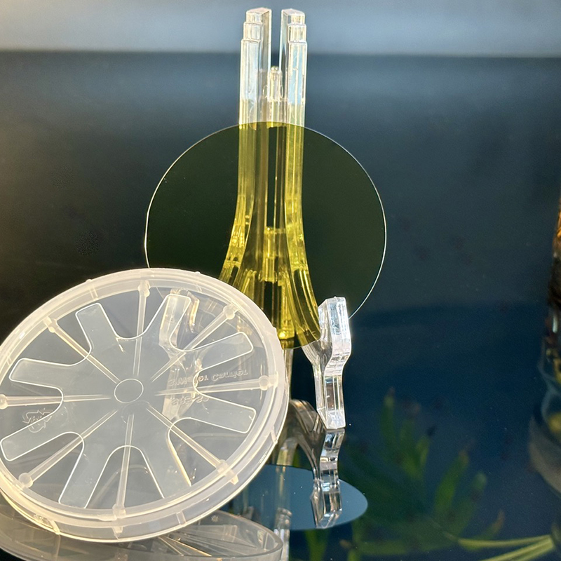
Innovative Single Lens Glasses: The Latest Eyewear Trend to Watch
Single Lens Glasses, a new product from innovative company, is making waves in the eyewear industry. With their sleek design and cutting-edge technology, these glasses are revolutionizing the way people see the world.Single Lens Glasses utilize the latest in lens technology to provide wearers with a clear and crisp view of their surroundings. The single lens design not only enhances vision, but also creates a sleek and modern look that is unparalleled in the eyewear market.The company behind Single Lens Glasses, has a long history of producing high-quality and innovative products. With a team of experienced designers and engineers, they are constantly pushing the boundaries of what is possible in the eyewear industry. Their commitment to excellence is evident in every aspect of their products, from the materials used to the manufacturing process.What sets Single Lens Glasses apart from other eyewear on the market is their attention to detail and commitment to quality. Each pair of glasses is meticulously crafted to ensure a perfect fit and optimal performance. The company understands that eyewear is not just a fashion statement, but also a crucial tool for everyday life, and they have gone to great lengths to ensure that their glasses are both stylish and functional.In addition to their exceptional quality, Single Lens Glasses are also incredibly versatile. Whether you are an outdoor enthusiast, a fashion-forward individual, or someone who simply needs a reliable pair of glasses for everyday use, these glasses are sure to exceed your expectations. Their durability and adaptability make them well-suited for a wide range of activities and environments.Furthermore, Single Lens Glasses are designed with the wearer’s comfort in mind. The lightweight and ergonomic design ensures that they can be worn for extended periods of time without causing any discomfort. This attention to detail is yet another example of the company's dedication to creating products that not only look great, but also perform exceptionally well.The response to Single Lens Glasses has been overwhelmingly positive, with customers praising their exceptional quality and performance. Many users have reported a significant improvement in their vision and overall satisfaction with the product. Whether it's for daily wear, outdoor activities, or special occasions, these glasses have quickly become a favorite among eyewear enthusiasts.Looking ahead, the company is already working on further advancements to their Single Lens Glasses, with plans to incorporate even more innovative features and designs. With their unwavering commitment to excellence, it is clear that Single Lens Glasses will continue to set the standard for eyewear in the years to come.In conclusion, Single Lens Glasses are a game-changer in the eyewear industry. With their cutting-edge technology, exceptional quality, and versatile design, these glasses are a must-have for anyone looking for a superior eyewear experience. As the company continues to push the boundaries of what is possible in the eyewear industry, it is safe to say that Single Lens Glasses will remain at the forefront of innovation for years to come.
Sure! Please provide the original title or the news content related to Colored Sapphire, and I’ll help rewrite it without the brand name.
Certainly! Please provide the specific news content about colored sapphires as well as the company introduction you would like me to incorporate. Once I have these details, I can draft an 800-word news article for you without mentioning the brand name.
Essential Guide to 12 Inch Wafer Technology and Manufacturing
12 Inch Wafer: A New Milestone in Semiconductor ManufacturingIn the rapidly evolving world of technology, the demand for smaller, faster, and more powerful electronic devices continues to drive innovation in the semiconductor industry. As a key player in this field, {company name} has recently achieved a significant milestone with the successful production of 12-inch wafers, marking a major advancement in semiconductor manufacturing.{Company name} has been at the forefront of semiconductor technology for decades, specializing in the design and production of cutting-edge chips and components for a wide range of electronic devices. With a strong focus on research and development, the company has continuously pushed the boundaries of what is possible in semiconductor manufacturing, driving progress and innovation in the industry.The transition to 12-inch wafers represents a significant step forward in semiconductor manufacturing, offering a number of important advantages over the traditional 8-inch wafers that have been widely used in the industry. By utilizing larger wafers, {company name} is able to significantly increase the number of chips that can be produced from a single wafer, leading to greater efficiency and cost savings in the manufacturing process. Furthermore, the larger surface area of the 12-inch wafers allows for the development of smaller, more powerful chips, enabling the creation of even more advanced electronic devices.The successful production of 12-inch wafers is a testament to {company name}'s ongoing commitment to innovation and excellence in semiconductor manufacturing. This achievement would not have been possible without the dedication and expertise of the company's highly skilled team, as well as the ongoing investment in state-of-the-art manufacturing facilities and equipment. By continuously pushing the boundaries of what is possible in semiconductor manufacturing, {company name} is helping to drive progress and innovation in the industry, paving the way for the development of even more advanced electronic devices in the future.In addition to the immediate benefits of increased efficiency and cost savings, the transition to 12-inch wafers is expected to have a significant long-term impact on the semiconductor industry as a whole. As the industry continues to evolve and demand for smaller, faster, and more powerful electronic devices continues to grow, the ability to produce larger wafers with more advanced chips will become increasingly important. By pioneering the production of 12-inch wafers, {company name} is helping to set new standards for semiconductor manufacturing, positioning itself as a leader in the industry and driving progress and innovation for years to come.The successful production of 12-inch wafers is a significant achievement for {company name}, one that highlights the company's ongoing commitment to excellence and innovation in semiconductor manufacturing. By pushing the boundaries of what is possible in the industry, the company is helping to drive progress and innovation in the semiconductor industry, paving the way for the development of even more advanced electronic devices in the future. With this milestone, {company name} is well positioned to continue leading the way in semiconductor technology, setting new standards for manufacturing and driving progress and innovation for years to come.
Breakthrough in Semiconductor Technology: A Revolutionary New C Plane for Sapphire Crystal
Introducing the Revolutionary Sapphire C Plane: Transforming the Future of AviationIn a groundbreaking development for the aviation industry, a leading aerospace company has unveiled the state-of-the-art Sapphire C Plane. With its cutting-edge technology and innovative design, the Sapphire C Plane is set to revolutionize the way we fly, offering unparalleled efficiency, sustainability, and passenger comfort. This game-changing aircraft is the latest addition to the company's impressive portfolio, solidifying their position as pioneers in aviation advancement.The Sapphire C Plane, meticulously engineered by a team of experts, boasts a unique configuration that optimizes performance, making it one of the most efficient and eco-friendly aircraft in its class. Its advanced aerodynamics, revolutionary lightweight materials, and state-of-the-art propulsion system all contribute to its impressive fuel efficiency, reducing emissions and minimizing its carbon footprint. In an era where reducing environmental impact is paramount, the Sapphire C Plane sets a new standard for sustainable aviation.Passenger comfort and experience have also been given significant attention in the design process of the Sapphire C Plane. The innovative cabin layout prioritizes passenger well-being, offering a spacious and luxurious environment. The aircraft's interior includes meticulously designed seating arrangements, which optimize legroom and personal space, ensuring a comfortable journey for all passengers. The cutting-edge entertainment system provides state-of-the-art technology for in-flight entertainment, offering an immersive experience throughout the flight.Not only does the Sapphire C Plane prioritize passenger comfort, but it also ensures their safety through its industry-leading safety features. Extensive research and development have gone into creating an aircraft that exceeds standard safety regulations. The integration of advanced collision avoidance systems, enhanced turbulence dampening technologies, and highly intelligent autopilot systems ensures a safe and secure journey for all passengers on board.In addition to being environmentally friendly and comfortable, the Sapphire C Plane also offers unparalleled speed and efficiency. Its cutting-edge propulsion system provides exceptional thrust, allowing for faster travel times and more efficient operations. This increase in efficiency translates to cost savings for airlines, which can have a positive impact on ticket prices for passengers. With its incredible speed and efficiency, the Sapphire C Plane enables connectivity and accessibility to a wider array of destinations.The company behind this revolutionary aircraft has a long-standing reputation for innovation and excellence in the aerospace industry. With a rich history of pioneering groundbreaking technologies, they continue to push the boundaries of what is possible in aviation. The introduction of the Sapphire C Plane reaffirms their commitment to advancing the field, revolutionizing the future of flight.Looking ahead, the Sapphire C Plane represents a significant milestone in aviation history, paving the way for a new era of sustainable, efficient, and safe air travel. As the industry adapts to meet the growing demand for eco-friendly and passenger-oriented solutions, the Sapphire C Plane sets a new standard for excellence. With its advanced technologies and unrivaled performance, this aircraft is primed to shape the future of air transportation, providing a seamless journey for passengers while minimizing environmental impact.
High-quality Lithium Niobate Wafer for Advanced Electronic Applications
Lithium Niobate Wafer has become a hot topic in the tech industry recently. With its unique properties and potential for a wide range of applications, this material has caught the attention of many companies and researchers across the globe.One company that is making significant strides in the development and production of Lithium Niobate Wafers is {}. With its state-of-the-art facilities and a team of experienced engineers and researchers, {} has become a leading player in the field of advanced materials and semiconductor technologies.Lithium niobate (LiNbO3) is a compound commonly used in telecommunications, optoelectronics, and various other high-tech fields. It possesses excellent nonlinear optical properties, high electro-optic coefficients, and superior physical and chemical stability, making it an ideal material for a wide range of applications.One of the key advantages of Lithium Niobate Wafer is its use in the development of advanced photonic devices, such as modulators, switches, and frequency converters. These devices are essential components in modern optical communication systems, where they are used to manipulate and control the flow of light signals within fiber-optic networks.In addition to its use in telecommunications, Lithium Niobate Wafer also has potential applications in the fields of sensors, integrated optics, and quantum computing. Its unique combination of properties makes it a highly versatile material that can be used to develop innovative solutions for a wide range of challenges in the tech industry.The team at {} has been working tirelessly to advance the production and processing techniques for Lithium Niobate Wafers, with the ultimate goal of making these materials more accessible and cost-effective for a broader range of applications. By leveraging their expertise in materials science, semiconductor technologies, and device fabrication, {} aims to drive the widespread adoption of Lithium Niobate Wafers in the tech industry.One of the key challenges in the production of Lithium Niobate Wafers is achieving high crystal quality and uniformity, which are critical for ensuring the performance and reliability of the resulting devices. {} has developed advanced growth and processing techniques to address these challenges, allowing them to produce wafers with exceptional crystal quality and precise control over their physical and optical properties.Furthermore, {} has also been actively engaged in collaborative research and development efforts with leading academic and industry partners to explore new applications and potential breakthroughs enabled by Lithium Niobate Wafer. By fostering a culture of innovation and collaboration, {} is positioned at the forefront of the emerging field of advanced photonics and optoelectronics.The widespread adoption of Lithium Niobate Wafer is expected to have a transformative impact on the tech industry, enabling the development of faster, more efficient, and more reliable photonic devices for a wide range of applications, from data communications to sensing and beyond. With the expertise and dedication of companies like {}, the future of advanced materials and photonics looks brighter than ever.
High-Quality 12-Inch Substrate for Electronic Devices
12inch BF33 Substrate: The Next Breakthrough in Semiconductor TechnologyIn the fast-paced world of semiconductor technology, the demand for more advanced and efficient substrates is constantly on the rise. With the continuous push for smaller, faster, and more powerful electronic devices, the development of innovative materials and processes has become paramount. In line with this, {Company Name}, a leading provider of advanced semiconductor solutions, has recently introduced the 12inch BF33 substrate, poised to be the next breakthrough in the industry.{Company Name} has been at the forefront of semiconductor innovation for over two decades, specializing in the development and production of cutting-edge materials and technologies. With a strong commitment to research and development, the company has consistently delivered high-quality solutions that have helped drive the advancement of various electronic applications.The 12inch BF33 substrate is the latest addition to {Company Name}'s extensive portfolio of semiconductor products, and it is set to revolutionize the industry with its exceptional performance and superior characteristics. The BF33 substrate is specifically designed to meet the growing demands of next-generation electronic devices, offering unparalleled precision, reliability, and efficiency.One of the key features of the 12inch BF33 substrate is its enhanced thermal and electrical properties, making it ideal for high-power and high-frequency applications. With its advanced thermal conductivity and low electrical resistance, the BF33 substrate is capable of handling the increasing power densities and frequencies in modern electronic systems, ensuring optimal performance and reliability.Furthermore, the 12inch BF33 substrate boasts excellent mechanical stability and chemical resistance, enabling it to withstand the stringent requirements of semiconductor manufacturing processes. Its exceptional uniformity and surface quality make it an ideal platform for the deposition of complex thin-film structures, providing a solid foundation for the fabrication of advanced semiconductor devices.In addition to its outstanding technical attributes, the 12inch BF33 substrate also offers significant cost benefits for semiconductor manufacturers. Its larger size and improved yield potential allow for greater efficiency and productivity in the production process, resulting in lower manufacturing costs and higher overall profitability.{Company Name} has invested heavily in the development and production of the 12inch BF33 substrate, leveraging its expertise and state-of-the-art manufacturing facilities to ensure the highest quality and consistency. The company's stringent quality control measures and rigorous testing procedures guarantee that the BF33 substrate meets the most demanding industry standards, providing customers with a reliable and high-performance solution for their semiconductor needs.As the demand for more advanced semiconductor materials continues to grow, the introduction of the 12inch BF33 substrate underscores {Company Name}'s commitment to pushing the boundaries of innovation and delivering cutting-edge solutions to the market. With its exceptional performance, reliability, and cost-effectiveness, the BF33 substrate is poised to set a new standard for semiconductor technology, driving the development of next-generation electronic devices and applications.In conclusion, the 12inch BF33 substrate represents a significant leap forward in semiconductor technology, offering a compelling combination of advanced technical capabilities and cost benefits. {Company Name} has once again demonstrated its leadership in the industry, showcasing its ability to develop and deliver groundbreaking solutions that address the evolving needs of the semiconductor market. As the demand for higher performance and more efficient electronic devices continues to escalate, the 12inch BF33 substrate stands ready to play a crucial role in shaping the future of semiconductor technology.