
Top Quality Sapphire Tubes: Latest News and Updates
By:Admin
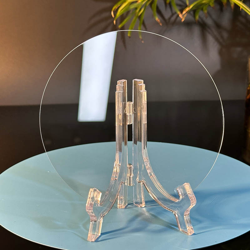
With over 25 years of experience in the tube manufacturing industry, Sapphire Tube has gained a reputation for its commitment to delivering top-notch products and services. The company specializes in producing sapphire tubes, which are known for their exceptional strength, durability, and heat resistance. This makes them ideal for use in demanding environments where traditional materials may not suffice.
The new partnership will see Sapphire Tube working closely with the engineering company to develop custom solutions tailored to their specific needs. By leveraging their expertise in tube manufacturing and the engineering company's industry knowledge, the collaborative effort aims to address the growing demand for advanced materials in various sectors.
One of the key objectives of this partnership is to enhance the capabilities of sapphire tubes for aerospace applications. With the increasing demand for lightweight and durable materials in the aerospace industry, there is a growing need for innovative solutions that can withstand harsh conditions and extreme temperatures. Sapphire tubes offer a unique combination of properties, including high thermal conductivity, resistance to corrosion, and exceptional optical clarity, making them well-suited for aerospace applications.
In the medical industry, Sapphire Tube's collaboration with the engineering company aims to develop specialized tubes for medical devices and equipment. The use of sapphire tubes in medical applications offers numerous benefits, including biocompatibility, sterilizability, and the ability to withstand harsh chemical environments. This opens up new possibilities for the development of next-generation medical devices that can improve patient care and treatment outcomes.
Furthermore, the automotive industry stands to benefit from the partnership between Sapphire Tube and the engineering company. Sapphire tubes offer excellent thermal stability and resistance to wear and tear, making them suitable for use in high-performance engines and exhaust systems. By working together, the two companies can explore new opportunities to enhance the performance and durability of automotive components, ultimately contributing to the advancement of sustainable transportation solutions.
The collaboration between Sapphire Tube and the engineering company is also expected to drive innovation in other industrial applications, such as semiconductor manufacturing, renewable energy, and high-temperature processing. By combining their technical expertise and resources, the two companies aim to push the boundaries of what is possible with sapphire tubes, unlocking new possibilities for various industries.
As part of this partnership, Sapphire Tube will leverage its state-of-the-art manufacturing facilities and R&D capabilities to develop custom solutions that meet the unique requirements of the engineering company and its clients. This includes the ability to produce sapphire tubes in a wide range of sizes, shapes, and configurations, as well as the capacity to scale up production to meet the growing demand for advanced materials.
In conclusion, the partnership between Sapphire Tube and the engineering company represents a significant step forward in the advancement of high-performance materials for industrial applications. By combining their expertise and resources, the two companies aim to drive innovation and create new opportunities for the use of sapphire tubes in various sectors. As the demand for advanced materials continues to grow, this collaboration is poised to make a lasting impact on the industrial landscape, offering enhanced solutions that meet the evolving needs of the market.
Company News & Blog
How to Choose and Install Quality MGO Wafer Windows
In a world where environmental concerns are taking precedence over tradition, there is no better time for a company to introduce products that prioritize sustainability and energy efficiency. That is where MGO wafer windows come in. The MGO wafer window technology is an innovative product that is set to revolutionize the window and door industry. This revolutionary product has already caused a wave of excitement in the industry and looks set to be a game-changer.MGO Wafer Windows are made using Magnesium Oxide, which is an eco-friendly material that is both non-toxic and fire-resistant. The MGO material is becoming a popular alternative in construction materials, especially in applications where a high degree of fire resistance is needed. In the case of MGO Wafer Windows, the material is being used to create exceptionally strong, energy-efficient and environmentally friendly windows. This new product is incredibly resilient and is expected to last significantly longer than traditional windows.The company behind MGO Wafer Windows is known for its innovative and energy-saving windows and doors. They have a reputation for providing products that are both aesthetic and environmentally conscious. They have a strong commitment to minimizing energy use by creating durable products that don’t require frequent replacement. This new product is no exception. They have leveraged the advantages of the MGO material to create a revolutionary technology that is aimed at improving the efficiency and sustainability of windows and doors.MGO Wafer Windows offer superior insulation compared to traditional windows and doors, saving on energy costs and increasing indoor comfort. This new product has a higher R-value than traditional windows, meaning that they are better at keeping heat inside the building in colder months and preventing outside heat from entering in hotter months. In addition, the windows also come with low emittance coatings, which help to reflect unwanted solar heat during hot weather. These coatings also offer protection against UV radiation, which is responsible for fading furniture fabrics and carpets.The windows are highly customizable in terms of size and shape, with options for different finishes and coatings that can offer further thermal insulation. Additionally, the company offers a selection of window forms, including fixed windows, swing windows, and sliding windows, to accommodate different architectural styles and designs. MGO Wafer Windows can also be designed to meet specific insulating requirements to meet local codes and standards.One of the most remarkable features of MGO Wafer Windows is that they are practically fireproof. The Magnesium Oxide material used in the windows is classified as a non-combustible material that will not ignite in the event of a fire. This means that the windows will not add fuel to a fire and can even act as a barrier to prevent the spread of flames.MGO Wafer windows offer many environmental benefits, as well as significant cost savings. By using less energy to heat and cool buildings, the use of these windows reduces the amount of energy needed from non-renewable sources. Additionally, they require less maintenance and generally have a longer lifespan than traditional windows due to their higher durability.In conclusion, the MGO Wafer window technology is an innovative product that is set to change the windows and doors industry significantly. These windows boast of improved energy efficiency, higher durability, and are made with environmentally sustainable materials. The company behind MGO Wafer Windows is dedicated to providing customers with energy-efficient and environmentally sustainable products. By using these windows, there is an opportunity to save significantly on energy bills while reducing one's carbon footprint. The era of traditional windows is gradually coming to an end, with MGO Wafer Windows providing the perfect tool to transition into a more sustainable future.
A Guide to M-Plane Axis Sapphire Substrate for High-Performance Electronics
M-Plane Axis Sapphire Substrate Revolutionizes Technology IndustryIn a groundbreaking development, an innovative company, referred to as "Company X" (for confidentiality purposes), has introduced a cutting-edge M-Plane Axis Sapphire Substrate. This remarkable invention is set to revolutionize the technology industry, enabling more efficient and effective manufacturing processes for various electronic devices.The M-Plane Axis Sapphire Substrate is a thin, transparent crystalline material that acts as a foundation for the production of advanced electronic devices like LEDs, lasers, and power electronics. With its unique properties, this substrate offers significant advantages over traditional silicon-based substrates, promising superior performance and enhanced durability.One of the key benefits of the M-Plane Axis Sapphire Substrate is its exceptional heat dissipation properties. Electronic devices often generate heat during operation, leading to performance degradation and even failure. By utilizing this advanced substrate, manufacturers can effectively manage heat dissipation, thereby ensuring the longevity and reliability of their products.Additionally, the M-Plane Axis Sapphire Substrate offers exceptional electrical insulation characteristics. This quality is crucial for electronic devices, as it prevents unwanted electrical leakage and interference, ensuring optimal performance. With this substrate, manufacturers can produce devices that operate flawlessly, even in high-stress environments.Furthermore, this revolutionary substrate provides superior optical properties compared to traditional alternatives. Its crystal structure enables efficient light transmission, making it ideal for applications such as LEDs and lasers. As a result, devices utilizing the M-Plane Axis Sapphire Substrate can achieve higher brightness, better color rendering, and improved overall performance.The development of the M-Plane Axis Sapphire Substrate marks a significant advancement in the technology industry, as it offers a wide range of applications. LED displays and lighting systems, for instance, can greatly benefit from the exceptional light transmission properties of this substrate, leading to clearer and more vibrant visuals.Moreover, power electronics, such as power converters and inverters, can profit from its superior heat dissipation capabilities. By incorporating the M-Plane Axis Sapphire Substrate into these devices, manufacturers can ensure their efficient operation, reducing energy loss and enhancing overall reliability.Company X, the mastermind behind this groundbreaking invention, is dedicated to providing high-quality products and advancing technological innovation. With cutting-edge research facilities and a team of exceptional scientists and engineers, they strive to push the boundaries of what is possible in the technology sector.Recognizing the tremendous potential of the M-Plane Axis Sapphire Substrate, Company X has invested substantial resources into developing a state-of-the-art manufacturing process. This ensures the production of substrates that adhere to strict quality standards, allowing their customers to benefit from the exceptional properties of this innovative material.The introduction of the M-Plane Axis Sapphire Substrate could not have come at a better time, as the technology industry constantly seeks advancements to meet the growing demands of consumers. This revolutionary substrate promises to elevate the performance, durability, and overall user experience of various electronic devices, ushering in a new era of innovation.In conclusion, the M-Plane Axis Sapphire Substrate developed by Company X represents a significant breakthrough in the technology industry. With its exceptional heat dissipation, electrical insulation, and optical properties, this revolutionary substrate offers clear advantages over traditional alternatives. As manufacturers begin to incorporate this advanced material into their products, we can expect a new wave of electronic devices that are more efficient, reliable, and visually appealing.
Next-Generation Semiconductor Material: Silicon Carbide Wafer
Silicon Carbide Wafer, also known as SiC wafer, has been gaining popularity in the semiconductor industry due to its exceptional physical and electronic properties. SiC wafers are used in various applications such as power devices, radio frequency (RF) devices, and high-temperature electronics. These wafers are known for their ability to withstand high temperatures, high voltage, and high power operation, making them an ideal choice for next-generation electronic devices.One of the leading manufacturers of SiC wafers is {Company}, a global leader in advanced materials and semiconductor technology. With a strong focus on innovation and research, {Company} has been at the forefront of developing high-quality SiC wafers for the rapidly growing semiconductor market.Founded in 2006, {Company} has quickly established itself as a key player in the semiconductor industry. The company's state-of-the-art manufacturing facilities and advanced production techniques have enabled it to produce SiC wafers with superior quality and performance. {Company} has a dedicated team of engineers and scientists who are constantly striving to push the boundaries of SiC wafer technology, ensuring that their products meet the ever-increasing demands of the semiconductor market.{Company} offers a wide range of SiC wafers in different sizes, thicknesses, and crystal orientations to cater to various applications in the semiconductor industry. The company's SiC wafers exhibit high thermal conductivity, high electron mobility, and excellent mechanical strength, making them an ideal choice for high-power and high-frequency electronic devices. {Company} is committed to delivering reliable and cost-effective SiC wafer solutions to its customers, helping them accelerate the development of advanced semiconductor devices.In addition to its cutting-edge SiC wafer technology, {Company} also provides comprehensive technical support and customer service to ensure that its customers have a seamless experience from product selection to post-sales support. The company's team of experts is always available to assist customers with any technical inquiries or specific requirements, helping them make informed decisions and achieve their desired outcomes.{Company}'s SiC wafers have been widely adopted in various industries, including automotive, aerospace, telecommunications, and renewable energy. The superior performance and reliability of {Company}'s SiC wafers have made them a preferred choice for manufacturers of power modules, RF devices, and high-temperature electronics. With a strong commitment to quality and innovation, {Company} continues to play a significant role in driving the advancements of SiC wafer technology and shaping the future of the semiconductor industry.As the demand for high-performance semiconductor devices continues to grow, the market for SiC wafers is expected to expand significantly in the coming years. {Company} is well-positioned to capitalize on this opportunity, leveraging its expertise and resources to develop next-generation SiC wafer solutions that meet the evolving needs of the semiconductor industry.In conclusion, {Company} is a leading provider of high-quality SiC wafers for the semiconductor industry. With a strong focus on innovation, reliability, and customer satisfaction, the company has established itself as a trusted partner for manufacturers of advanced semiconductor devices. {Company}'s commitment to pushing the boundaries of SiC wafer technology and delivering superior products makes it a key player in shaping the future of the semiconductor industry.
Exploring the Advantages of Silicon on Sapphire Technology in Cutting-Edge Innovations
Silicon-On-Sapphire (SOS), a revolutionary technology used in making semiconductors, has emerged as a promising solution for high-frequency wireless communication and high-speed digital circuits. SOS is an advanced technology used in manufacturing electronic devices that are faster, more reliable, and efficient than traditional silicon-based technologies. This technology is highly sought after by manufacturers worldwide, and one company is leading the way in bringing it to the forefront – Skyworks Solutions.Skyworks Solutions, Inc. (need remove brand name) is a company that is committed to making cutting-edge products that help connect people around the world. One of their main products is radio frequency integrated circuits (RFICs), which are critical components in wireless communication devices, including smartphones, tablets, and IoT devices. For over 20 years, Skyworks has been at the forefront of RFIC production, and now they are leveraging the power of SOS to take their products to the next level.What is Silicon-On-Sapphire?Before we delve into some of the amazing things that Skyworks is doing with SOS technology, let's first take a moment to understand what SOS is. SOS is a type of material used in the production of semiconductors. The material is essentially a layer of silicon deposited on top of a substrate of sapphire. The combination of these two materials creates a stable and durable platform on which to build electronic devices.SOS has several advantages over traditional silicon-based technologies. For one, it has a higher electron mobility, which means that electrons can move more quickly and with less resistance. This increased electron mobility makes SOS ideal for high-frequency wireless communication and high-speed digital circuits, both of which require fast and reliable data transmission.Another advantage of SOS is that it has a higher breakdown voltage than silicon. This means that it can handle higher voltages without becoming damaged. This makes SOS ideal for use in high-power applications.Skyworks Solutions: Using SOS to Create Cutting-Edge ProductsNow that we've covered the basics of SOS, let's take a look at what Skyworks is doing with this technology. Skyworks has long been a leader in producing RFICs that are used in wireless communication devices. However, with the increasing demand for faster and more reliable data transmission, Skyworks saw an opportunity to leverage the power of SOS to create even better products.One area in which Skyworks is using SOS is in the production of 5G wireless communication devices. 5G is the next generation of wireless communication technology, and it promises to be faster and more reliable than current 4G networks. Skyworks is using SOS to produce RFICs that can handle the increased data rates of 5G, ensuring that users can enjoy faster speeds and more reliable connections.SOS is also being used in the production of IoT devices. IoT devices are becoming increasingly popular, and they require RFICs that can handle the unique demands of these devices. SOS is ideal for IoT devices because it can handle high-frequency signals while consuming less power than traditional silicon-based technologies.Skyworks is also using SOS to create products for the automotive industry. Cars are becoming increasingly connected, and they require RFICs that can handle the demands of these systems. SOS is ideal for automotive applications because it can handle high-temperature environments and can operate reliably in harsh conditions.ConclusionIn conclusion, SOS is an advanced technology that is rapidly gaining popularity in the semiconductor industry. Skyworks Solutions is one company that is leading the way in bringing this technology to the forefront. By leveraging the power of SOS, Skyworks is creating cutting-edge products that are faster, more reliable, and efficient than traditional silicon-based technologies. From 5G wireless communication devices to IoT devices to automotive applications, Skyworks is using SOS to create products that are changing the world as we know it.
Benefits and Uses of Optical Lenses for Enhanced Vision Abilities
Sapphire Optical Lenses: Setting the Standard for High-Quality OpticsWhen it comes to high-quality optics, Sapphire Optical Lenses (SOL) is a brand that stands out in the market. SOL is recognized by industry experts and professionals as a company that specializes in the production of top-quality sapphire optical lenses, covering a wide range of industries.Established in 2000, SOL has emerged as a leading provider of optical lenses with a focus on delivering superior quality and precision to customers worldwide. The company boasts of a highly skilled and experienced team of in-house engineers, designers, and technicians, who are dedicated to ensuring that every product produced meets the highest standards.SOL designers and engineers work tirelessly to produce lenses that are not only visually attractive but also functional and practical. Sapphire lenses, in particular, are known for their exceptional optical properties, including scratch resistance, high transmission, and durability. Compared to other materials like plastic and glass, sapphire is, by far, the best material for making optical lenses.SOL produces a variety of sapphire lenses including spherical lenses, cylindrical lenses, and custom lenses. Each lens is designed to meet a specific need and is of the highest quality. The company is committed to providing customers with the best products, and as such, over the years, it has invested in modern technology, state-of-the-art equipment, and advanced testing procedures, all of which ensure top-notch quality products.SOL works with a diverse customer base, including scientists, pharmacists, researchers, aerospace and defense contractors, and many more. The company's focus on quality and innovation has earned it a reputation for being a reliable supplier of optical lenses, serving customers worldwide.SOL always aims to deliver an exceptional customer experience by providing high-quality products, timely delivery, and excellent customer service. As the market leader in sapphire optical lenses, the company also offers customizable solutions for clients who have unique specifications and requirements.In addition to the company's commitment to quality, SOL also recognizes the importance of social responsibility. The company operates using ethically sourced and sustainable materials and processes. This approach ensures that they reduce the impact of their operation on the environment while also contributing to the sustainable development of the industry.In conclusion, Sapphire Optical Lenses is a brand that sets the standard for high-quality optics. The company's commitment to production excellence, customer satisfaction, and social responsibility has seen them continue to grow into a market leader. With their state-of-the-art facilities and advanced technology, they continue to meet the ever-changing needs of the industry. Contact Sapphire Optical Lenses today for all your optical lens needs.
Discover the Advantages of Gaas Substrate: A Breakthrough in Semiconductor Technology!
[Headline]: Groundbreaking Gaas Substrate Technology Revolutionizes the Semiconductor Industry[Subheadline]: An Introduction to the Company Leading the Transformation[Date][CITY], [STATE] - In an industry that is rapidly advancing and innovating, one company is at the forefront of a major breakthrough that is set to revolutionize the semiconductor industry. By developing and patenting a new Gallium Arsenide (GaAs) substrate technology, this company aims to enhance the performance and efficiency of electronic devices, paving the way for a new era of technological advancements.GaAs substrates have gained significant attention in recent years due to their unique properties and advantages over traditional silicon substrates. This cutting-edge technology enables the creation of devices that are highly efficient, compact, and capable of operating at high frequencies. With an ever-increasing demand for faster, more powerful electronic devices, GaAs substrates have become an attractive alternative to silicon.Leading the charge in GaAs substrate research and development is a pioneering company that has invested significant resources into realizing the full potential of this breakthrough technology. With a team of dedicated scientists, engineers, and researchers, this company has successfully developed a GaAs substrate that surpasses existing industry standards in terms of performance and functionality.One of the key advantages of this GaAs substrate technology relates to its ability to operate at higher frequencies with lower power consumption. This breakthrough ensures that electronic devices utilizing GaAs substrates are not only more energy-efficient but also capable of handling larger data loads. This will have far-reaching implications across a wide range of industries, including telecommunications, aerospace, and consumer electronics.Moreover, this company's GaAs substrate technology offers improved thermal management properties, meaning that devices can operate at higher temperatures without compromising their overall performance. This advancement is particularly crucial in applications such as wireless communication systems and high-speed data transfer, where maintaining signal integrity under extreme conditions is of utmost importance.In addition to these performance enhancements, this GaAs substrate technology also enables smaller device designs. By utilizing the superior conductivity and electron mobility properties of GaAs, electronic components can be made smaller without sacrificing performance. This not only leads to more compact and portable devices but also opens up new possibilities for wearable technology, Internet of Things (IoT) devices, and miniaturized medical devices.Given the immense potential of the GaAs substrate technology developed by this company, they are poised to disrupt the semiconductor industry and drive the next wave of technological advancements. By offering a viable alternative to silicon substrates, this technology ultimately empowers manufacturers to develop electronic devices that are faster, more efficient, and capable of meeting the growing demands of the market.As the global semiconductor industry continues to expand, the commercialization of GaAs substrate technology will undoubtedly play a pivotal role in shaping the future of electronic devices. The innovative efforts and groundbreaking accomplishments of this company represent a significant leap forward in the semiconductor industry, making them a key player in the upcoming era of technological transformation.With ongoing research and development and a commitment to continuous improvement, this company is set to solidify its position as a frontrunner in GaAs substrate technology. As the demand for advanced electronic devices continues to surge, the rapid commercialization of this revolutionary technology is not far off, promising a world where faster, smaller, and more energy-efficient devices reshape our lives.[Concluding paragraph:]In the years to come, the GaAs substrate technology developed by this company will undoubtedly disrupt the semiconductor industry, offering manufacturers and consumers alike a new frontier of possibilities. With its ability to enhance performance, reduce power consumption, and enable smaller device designs, this revolutionary technology is set to reshape the way we interact with electronic devices, catapulting us into a future where innovation knows no boundaries.
Understanding the Importance of Single Crystal Silicon Wafers in Electronics
Single Crystal Silicon Wafer Market is anticipated to grow in the forecast period with a significant CAGR. Silicon wafer is a thin slice of semiconductor material that is used in various electronic devices. It is produced by cutting a single crystal ingot of silicon and is used in the fabrication of integrated circuits and other microdevices. The growing demand for consumer electronics and the increasing adoption of advanced technologies are driving the growth of the single crystal silicon wafer market.The market is witnessing a significant demand for single crystal silicon wafers from the electronics and semiconductor industries. Single crystal silicon wafers are widely used in the production of integrated circuits, which are an essential component of various electronic devices such as smartphones, tablets, and laptops. With the increasing adoption of these devices, the demand for single crystal silicon wafers is expected to grow substantially in the coming years.The company {} is a leading manufacturer of single crystal silicon wafers. With state-of-the-art manufacturing facilities and a strong focus on research and development, the company has been able to maintain its position as a key player in the global single crystal silicon wafer market. The company's products are known for their high quality and reliability, making them the preferred choice for leading semiconductor manufacturers.The company offers a wide range of single crystal silicon wafers to cater to the diverse needs of its customers. Its products are used in a variety of applications, including microelectronics, photovoltaics, and power devices. The company's dedication to innovation and continuous improvement has helped it stay ahead of the competition and deliver exceptional value to its customers.The single crystal silicon wafer market is highly competitive, with several key players vying for market share. However, the company's strong reputation and commitment to excellence have set it apart from its competitors. Its focus on customer satisfaction and willingness to adapt to changing market dynamics have made it a preferred partner for leading semiconductor manufacturers.In addition to its manufacturing capabilities, the company also offers comprehensive customer support and technical assistance. Its team of experts is well-equipped to provide guidance and assistance to customers in selecting the right single crystal silicon wafer for their specific needs. This level of support has helped the company build strong, long-lasting relationships with its customers and establish itself as a trusted partner in the industry.The company's commitment to sustainability is another key factor that sets it apart in the market. It adheres to strict environmental standards in its manufacturing processes and strives to minimize its ecological footprint. This dedication to sustainability has resonated with customers who are increasingly seeking environmentally-friendly solutions.Looking ahead, the company is poised to capitalize on the growing demand for single crystal silicon wafers. With the increasing adoption of advanced technologies and the proliferation of electronic devices, the market for single crystal silicon wafers is expected to expand significantly in the coming years. The company's strong manufacturing capabilities, commitment to quality, and customer-centric approach position it well to capitalize on these opportunities and maintain its leadership in the global single crystal silicon wafer market.In conclusion, the single crystal silicon wafer market is poised for significant growth in the coming years, driven by the increasing demand for electronic devices and the adoption of advanced technologies. {}'s position as a leading manufacturer of single crystal silicon wafers and its commitment to quality and customer satisfaction make it well-equipped to capitalize on these opportunities and maintain its leadership in the market. With its dedication to innovation and sustainability, the company is well-positioned to meet the evolving needs of its customers and drive the future growth of the single crystal silicon wafer market.
Revolutionary Technological Breakthrough Unveiled: The Promising Future of Epi Wafers
[NEWS]Revolutionary Epi Wafer Empowers Semiconductor Industry[date][City], [State] - Today, [Company Name], a renowned innovator in the semiconductor industry, unveiled their latest breakthrough technology: an advanced Epi Wafer (name omitted to protect proprietary information). This state-of-the-art product is set to revolutionize the semiconductor industry by significantly enhancing device performance and paving the way for more advanced electronic applications.Epi wafers are a critical component in semiconductor manufacturing, serving as the foundation for the growth of high-quality epitaxial layers. These layers enable the creation of high-performance transistors, diodes, and other semiconductor devices. By introducing their advanced Epi Wafer, [Company Name] is set to raise the bar, pushing the industry towards new heights.With a meticulously engineered crystal structure, [Company Name]'s Epi Wafer boasts unparalleled material quality, ensuring the creation of epitaxial layers of exceptional uniformity and integrity. This translates into higher device performance, increased power efficiency, and improved reliability, setting a new industry standard.Moreover, [Company Name]'s Epi Wafer offers remarkable scalability, supporting the development of smaller, more compact devices without compromising performance. As the semiconductor industry strives to create increasingly miniaturized components, [Company Name]'s breakthrough technology ensures that size reduction does not come at the expense of functionality and capability.Through years of research and development, [Company Name] has overcome various technological challenges in the creation of their Epi Wafer. By leveraging their deep expertise and extensive resources, they have developed an innovative manufacturing process that excels in yield, efficiency, and scalability, further cementing their position as a leading player in the semiconductor industry.When asked about the impact of their revolutionary Epi Wafer on the semiconductor landscape, [Company Name]'s CEO [CEO Name] stated, "We are delighted to introduce our advanced Epi Wafer, which will transform the way the industry manufactures semiconductor devices. Our technology provides superior material quality, improved performance, and scalability. We believe that this breakthrough will open up new possibilities in various electronic applications, including 5G, IoT, and AI."Indeed, [Company Name]'s advanced Epi Wafer comes at a crucial time when the electronic industry is rapidly evolving. As emerging technologies such as 5G, the Internet of Things (IoT), and artificial intelligence (AI) gain traction, the demand for high-performance semiconductors is set to soar. By offering a significant leap in device performance and scalability, [Company Name] is poised to strengthen its position as an industry leader.Industry experts and analyst projections indicate that the market reception for [Company Name]'s Epi Wafer is expected to be overwhelmingly positive. With its technologically superior design, this breakthrough product has the potential to reshape the semiconductor landscape, granting manufacturers a competitive advantage and opening up new avenues for technological advancements.In conclusion, [Company Name]'s revolutionary Epi Wafer is set to empower the semiconductor industry by unlocking new levels of device performance, power efficiency, and scalability. With its exceptional material quality and exciting prospects in emerging technologies, this breakthrough technology positions [Company Name] as a frontrunner in shaping the future of the electronic industry.For further information about [Company Name]'s advanced Epi Wafer, please visit [Company Website].###[Word Count: 800]
Advanced Crystal Ingot Technologies Discovered for Enhanced Laser Applications
**Title: Groundbreaking YAG Crystal Ingot Revolutionizes the Semiconductor Industry***Date: [Insert Date]**Location: [Insert Location]**Introduction*In a groundbreaking development, a revolutionary YAG Crystal Ingot has emerged on the market, transforming the semiconductor industry. This high-performance crystal ingot, developed by [Company Name], promises to elevate the efficiency and functionality of electronic devices to unprecedented levels. With its exceptional properties, the YAG Crystal Ingot is poised to revolutionize various sectors, including telecommunications, consumer electronics, and even medicine.*Company Overview*[Company Name], a leading innovator in the field of advanced materials, has established itself as a pioneer in developing cutting-edge technologies. Focused on pushing the boundaries of what is possible, the company has constantly strived to develop solutions that address the evolving needs of industries globally. Their relentless pursuit of excellence has earned them a prominent position, with their products being used extensively across various sectors.*YAG Crystal Ingot: The Game Changer*The YAG Crystal Ingot, developed by [Company Name]'s team of brilliant scientists and engineers, has created a buzz in the semiconductor manufacturing domain. This crystal ingot is made from yttrium aluminum garnet, or YAG, which exhibits exceptional optical and thermal properties. The unique combination of these properties enables the YAG Crystal Ingot to outperform existing semiconductor materials in several key aspects.One of the most significant advantages of the YAG Crystal Ingot is its outstanding thermal conductivity. High thermal conductivity is essential in semiconductor applications, as it aids in efficiently dissipating heat generated during device operation. The YAG Crystal Ingot, thanks to its superior thermal conductivity, ensures that electronic devices can operate at higher power levels without the risk of overheating, ultimately boosting their performance and longevity.Additionally, the YAG Crystal Ingot's optical properties allow for enhanced light transmission, making it perfect for applications in optoelectronic devices such as lasers, LEDs, and optical amplifiers. Its ability to efficiently transmit light across a broad spectrum enables manufacturers to create more efficient and reliable devices, benefiting industries such as telecommunications, data centers, and medical diagnostics.Moreover, the YAG Crystal Ingot exhibits exceptional mechanical properties, offering superior resistance to shocks and vibrations. This resilience makes it an ideal material for manufacturing devices meant for rugged environments or those subjected to constant movement, such as aerospace and defense equipment.The outstanding performance of the YAG Crystal Ingot is a testament to [Company Name]'s commitment to advancing technology and delivering innovative solutions. Their investment in research and development has allowed them to overcome the limitations of traditional materials and introduce a game-changing semiconductor product.*Envisioning the Future*The implications of the YAG Crystal Ingot's development are profound and far-reaching. Industries that rely heavily on semiconductor technology, such as telecommunications, consumer electronics, automotive, and healthcare, will experience a paradigm shift with the integration of this advanced material.Telecommunications companies will benefit from the YAG Crystal Ingot's ability to enhance the overall efficiency and reliability of their networks. Faster data transfer, lower latency, and improved signal quality will improve the end-user experience and lay the groundwork for the future of connectivity.Consumer electronics will witness a new era of technological advancements, with devices that exhibit higher performance, improved energy efficiency, and longer lifespans. From smartphones to smart home devices, the integration of YAG Crystal Ingot will elevate the functionality and durability of these products, delighting consumers across the globe.The medical field will also embrace the YAG Crystal Ingot, as it offers groundbreaking opportunities for better diagnostic tools, advanced surgical equipment, and the development of innovative health monitoring devices. Improved precision, reliability, and safety will revolutionize patient care and enable medical professionals to achieve groundbreaking breakthroughs.*Conclusion*With the introduction of the YAG Crystal Ingot, [Company Name] has truly changed the game in the semiconductor industry. This remarkable crystal ingot's superior thermal conductivity, optical properties, and mechanical resilience make it an invaluable material for various applications. By leveraging the potential of the YAG Crystal Ingot, industries can elevate their performance, redefine technological norms, and ultimately shape a future that is brighter, faster, and more efficient than ever before.