
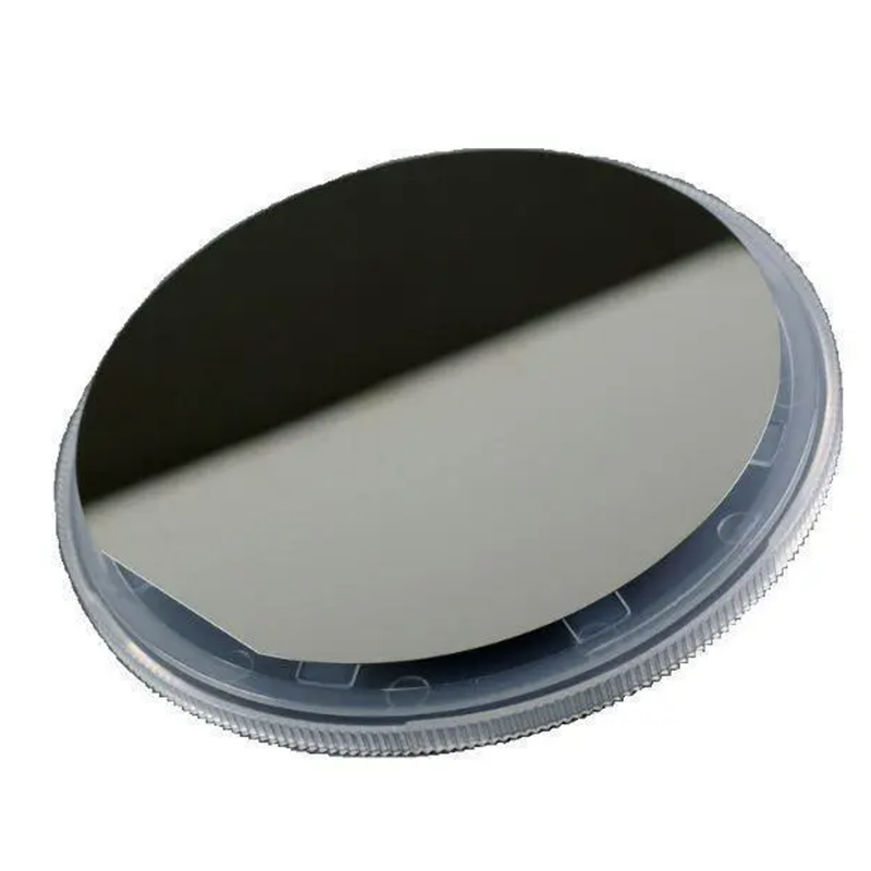
High-Quality Gallium Arsenide Wafers for Advanced Semiconductor Applications
By:Admin
Company News & Blog
High-Quality Watch Face Made of Sapphire Crystal
Sapphire Crystal Watch Face, a leader in the world of luxury timepieces, has recently unveiled its latest collection of watch faces that are sure to captivate watch enthusiasts worldwide. The company, known for its commitment to quality and innovation, has once again raised the bar with its newest offerings.With a history that spans over several decades, Sapphire Crystal Watch Face has established itself as a premier name in the watch industry. The company has built a reputation for crafting timepieces that are not only stylish and elegant but also durable and reliable. This commitment to excellence has earned Sapphire Crystal Watch Face a loyal following of customers who value superior craftsmanship and attention to detail.The latest collection of watch faces from Sapphire Crystal Watch Face is a testament to the company's dedication to pushing boundaries and setting new standards in the industry. Each watch face in the collection is meticulously crafted using the finest materials and cutting-edge technology. One of the standout features of the collection is the use of sapphire crystal, known for its exceptional hardness and scratch resistance. Not only does this material enhance the durability of the watch faces, but it also provides a clear and pristine surface that allows for easy readability.In addition to the use of sapphire crystal, the new collection showcases a range of designs that cater to different tastes and preferences. Whether it's a classic, minimalist look or a more contemporary and bold style, there is something for everyone in the collection. Each watch face is a testament to the company's commitment to versatility and innovation, ensuring that customers can find the perfect timepiece to complement their individual style.Furthermore, Sapphire Crystal Watch Face has also taken a step towards sustainability with the new collection. The company has implemented eco-friendly practices in the production of its watch faces, ensuring that each piece is made with a minimal environmental impact. This is part of the company's wider commitment to corporate responsibility and ethical manufacturing, a commendable initiative that resonates with customers who value sustainability and ethical business practices.The launch of the new collection has generated significant buzz within the watch industry, with experts and enthusiasts alike praising Sapphire Crystal Watch Face for its unwavering dedication to quality and innovation. In a market saturated with generic and uninspired offerings, the new collection stands out as a testament to the company's ability to push boundaries and set new trends.In a statement, the company's CEO expressed their excitement about the new collection, highlighting the hard work and dedication that went into creating it. "We are thrilled to introduce our latest collection of watch faces, which we believe showcase the very best of what Sapphire Crystal Watch Face has to offer," they said. "We have poured our hearts and souls into this collection, and we are confident that it will exceed the expectations of our customers."For watch enthusiasts and connoisseurs who appreciate craftsmanship and attention to detail, the new collection from Sapphire Crystal Watch Face is a testament to the company's commitment to excellence. With its use of sapphire crystal, diverse design options, and a focus on sustainability, the collection is a true reflection of the company's ethos, and a testament to its ongoing success in the world of luxury timepieces. As Sapphire Crystal Watch Face continues to push boundaries and set new standards, it is clear that the company will remain a dominant force in the industry for years to come.
Quality Science Laboratory Equipment for All Your Research Needs
Science Laboratory Equipment is a leading supplier of high-quality laboratory instruments and equipment for research, development, and quality control applications. With a focus on providing reliable and precise tools for scientific analysis, Science Laboratory Equipment has established itself as a trusted partner for laboratories across a wide range of industries.The company offers a comprehensive range of laboratory equipment, including but not limited to, pipettes, centrifuges, microscopes, balances, and spectrophotometers. These instruments are essential for conducting various experiments and tests in fields such as biology, chemistry, physics, and environmental science.Science Laboratory Equipment prides itself on delivering innovative and cutting-edge products that meet the evolving needs of modern laboratories. Its team of scientists and engineers is dedicated to developing and perfecting new technologies to enhance the efficiency and accuracy of laboratory processes.In addition to its commitment to quality and innovation, Science Laboratory Equipment places a strong emphasis on customer satisfaction. The company offers personalized support and guidance to help customers select the right equipment for their specific applications. Furthermore, Science Laboratory Equipment provides comprehensive training and technical assistance to ensure that customers can maximize the performance of their instruments.Recently, Science Laboratory Equipment unveiled its latest addition to its product line: a state-of-the-art spectrophotometer. This advanced instrument is designed to deliver exceptional performance and reliability, making it an invaluable tool for a wide range of scientific applications. With its user-friendly interface and powerful analytical capabilities, the new spectrophotometer is set to revolutionize the way laboratories conduct research and analysis.The spectrophotometer boasts a number of features that set it apart from other instruments on the market. Its high-resolution optics and advanced light source technology ensure accurate and reproducible results, even for the most demanding applications. Furthermore, the spectrophotometer is equipped with a range of automated functions that streamline the analytical process, saving time and reducing the risk of human error.One of the most exciting aspects of the new spectrophotometer is its compatibility with cloud-based data management systems. This feature allows users to seamlessly transfer and store their analytical data, enabling easy access and sharing across multiple devices and locations. Science Laboratory Equipment has also developed a dedicated mobile app that allows users to monitor and control the spectrophotometer remotely, providing unparalleled convenience and flexibility.The launch of the new spectrophotometer represents Science Laboratory Equipment's ongoing commitment to advancing scientific research and analysis. By providing laboratories with the latest technological innovations, the company aims to empower researchers and analysts to achieve new breakthroughs and discoveries in their respective fields.In addition to its product innovations, Science Laboratory Equipment continues to expand its global presence and reach. The company has established a strong network of distributors and partners around the world, enabling it to serve a diverse range of customers with varying needs and requirements. Science Laboratory Equipment also regularly participates in industry trade shows and exhibitions to showcase its products and connect with potential customers and collaborators.Looking ahead, Science Laboratory Equipment is dedicated to furthering its mission of providing cutting-edge laboratory instruments and equipment to support scientific progress. The company's commitment to quality, innovation, and customer satisfaction positions it as a leading force in the scientific instrumentation industry, and it is poised to continue driving advancements in laboratory technology for years to come.As the demand for high-quality laboratory equipment continues to grow, Science Laboratory Equipment stands ready to meet the needs of laboratories around the world. With its unparalleled expertise and dedication to excellence, the company is well-positioned to make a lasting impact on the scientific community and contribute to the advancement of knowledge and innovation.
Sapphire Ingot Production and Demand Soar as Market Embraces its Versatility
Title: Technological Advancements in Sapphire Ingot Production: A Breakthrough for the Semiconductor IndustryIntroduction:In recent years, the global semiconductor industry has experienced significant growth due to the increasing demand for advanced electronic devices. As this demand continues to rise, the need for reliable and high-quality raw materials, such as sapphire ingots, has become critical. To address this market demand, a leading technology company has unveiled a groundbreaking innovation in sapphire ingot production, revolutionizing the semiconductor industry.Technological Advancements:Traditionally, the production of sapphire ingots, which are widely used as a substrate material in the manufacturing of LEDs, power electronics, and high-frequency devices, has been a laborious and costly process. However, with the development of cutting-edge technology, this company has successfully perfected a highly efficient method to produce sapphire ingots, promising to meet the soaring demands of the industry.Through extensive research and collaboration with industry experts, engineers have developed a state-of-the-art manufacturing process that significantly improves sapphire ingot production. Combining advanced crystal growth techniques with innovative automation systems, the company has succeeded in increasing yield, reducing manufacturing costs, and maintaining consistent quality. This breakthrough technology has the potential to reshape the semiconductor industry's supply chain, enabling accelerated growth and innovation.Enhanced Crystal Growth Techniques:Among the key advancements lies the optimization of crystal growth techniques. With the help of precise temperature control and innovative seeding methodologies, the company has achieved higher crystalline quality, ensuring uniformity throughout the entire sapphire ingot. This enhanced crystal structure not only contributes to improved device performance but also reduces manufacturing defects, increasing yield and reducing waste.Furthermore, innovative automation systems have been implemented to streamline the production process. Robotic handling systems, coupled with advanced sensors and artificial intelligence, significantly reduce human intervention, leading to higher throughput and enhanced efficiency. This not only saves time but also mitigates the risk of human error.Benefits and Market Impact:The introduction of this advanced sapphire ingot production technique is poised to have a profound impact on the semiconductor market. The following benefits can be expected:1. Increased Supply: The improved efficiency in sapphire ingot manufacturing will result in higher production volumes, thus meeting the growing demand for semiconductors. This breakthrough will promote technological advancement across various industries, including consumer electronics, automotive, and telecommunications.2. Cost Reduction: The innovative process will contribute to a reduction in manufacturing costs, benefiting both manufacturers and consumers. The increased availability of cost-effective sapphire ingots will enable the development of more affordable electronic devices, thereby empowering a wider range of consumers to access cutting-edge technology.3. Environmental Sustainability: By optimizing the manufacturing process, the company also emphasizes environmental sustainability. Lower energy consumption and reduced material wastage contribute to a greener future during the production of sapphire ingots.Collaboration and Future Outlook:The successful implementation of this groundbreaking technology has been the result of ongoing collaboration within the semiconductor industry. The company actively engaged with research institutions, customer feedback, and industry experts to refine and improve the production process continually. This collaborative approach ensures that the technology remains at the forefront of innovation, positioning the company as a leader in the field.Looking ahead, the company plans to expand its production capacity, leveraging its breakthrough sapphire ingot manufacturing process. By adopting these advancements on a larger scale, the company aims to address the growing demand for semiconductor materials worldwide. In addition, ongoing research and development endeavors will focus on advancing crystal growth techniques further, enhancing the overall quality of sapphire ingots and enabling even more advanced semiconductor applications.Conclusion:The introduction of an advanced sapphire ingot production technique represents a significant milestone in the semiconductor industry. Through innovative crystal growth techniques and automation systems, this breakthrough technology promises increased supply, reduced costs, and environmental sustainability. Furthermore, continued collaboration and research will ensure the company remains at the forefront of technological advancement in the field of sapphire ingot manufacturing. These advancements will undoubtedly stimulate further growth and innovation across the entire semiconductor industry, ultimately benefitting consumers worldwide.
High-quality Germanium Wafers for Semiconductor Applications
Germanium Wafer Market is anticipated to reach XX% CAGR during 2021-2026. Germanium is a lustrous, hard, grayish-white metalloid in the carbon group with an atomic number of 32 in the periodic table. Germanium wafer is used in various applications such as infrared optics, solar cells, nanowires, and others.The Germanium Wafer market is expected to witness significant growth due to the increasing demand for consumer electronics and the adoption of advanced technologies in the industry. The rise in demand for infrared optics and solar cells is also driving the growth of the Germanium wafer market. Additionally, the growing use of Germanium in the production of nanowires for semiconductors and optoelectronics is expected to further boost the market growth.The global Germanium Wafer market is segmented based on type, application, and region. Based on type, the market is divided into N-type, P-type, and others. N-type Germanium wafers are widely used in the production of solar cells and infrared optics, while P-type Germanium wafers find applications in nanowires and semiconductors.On the basis of application, the market is categorized into consumer electronics, solar cells, infrared optics, nanowires, and others. The consumer electronics segment is expected to dominate the market due to the increasing use of Germanium wafers in smartphones, tablets, and other electronic devices. The solar cells segment is also anticipated to witness significant growth due to the increasing demand for renewable energy sources.Regionally, the Germanium Wafer market is segmented into North America, Europe, Asia Pacific, Latin America, and Middle East & Africa. Asia Pacific is expected to dominate the market due to the presence of major consumer electronics manufacturers in the region. The increasing investments in the solar energy sector in countries like China and India are also driving the market growth in the region. Europe and North America are also expected to witness substantial growth due to the growing demand for advanced technologies in the region.{Company Name} is one of the leading manufacturers of Germanium wafers in the market. The company offers a wide range of Germanium wafers with superior quality and performance. {Company Name} has a strong presence in the global market and has a solid customer base in various industries.The company's Germanium wafers are widely used in the production of semiconductor devices, infrared optics, and solar cells. {Company Name} has a state-of-the-art manufacturing facility, equipped with advanced technologies to produce high-quality Germanium wafers that meet the industry standards and customer requirements.{Company Name} is known for its commitment to innovation and continuous improvement. The company invests heavily in research and development to develop advanced Germanium wafer technologies and enhance its product portfolio. {Company Name} also focuses on sustainability and environmental protection by adopting eco-friendly manufacturing processes and reducing its carbon footprint.The company has a strong distribution network and a dedicated sales team to cater to the growing demand for Germanium wafers in the global market. {Company Name} is committed to providing excellent customer service and technical support to its clients and partners.In conclusion, the global Germanium Wafer market is poised for significant growth in the coming years due to the increasing demand for consumer electronics, solar cells, and advanced technologies. {Company Name} is well-positioned to capitalize on this growth with its high-quality Germanium wafers and strong market presence. With its focus on innovation, sustainability, and customer satisfaction, {Company Name} is set to play a key role in shaping the future of the Germanium wafer market.
How to Choose the Best Smartphone for Your Needs
GanThe company {} is making headlines once again as they launch their latest product that is set to revolutionize the industry. With a reputation for innovation and quality, {} has consistently delivered state-of-the-art products that have set the bar for excellence. Their newest offering, which is a result of years of research and development, promises to once again push boundaries and exceed expectations.{} has established itself as a leader in the industry, known for its commitment to excellence and its ability to adapt to the ever-changing needs of its customers. With a strong focus on research and development, the company has consistently produced cutting-edge products that have redefined the industry. Their latest product is no exception, as it represents the culmination of years of hard work and dedication to pushing the boundaries of what is possible.The new product, which is set to launch in the coming months, is expected to have a significant impact on the industry. With its innovative features and advanced technology, it is poised to set new standards for performance and reliability. Customers can expect a product that is not only highly effective but also easy to use and maintain, making it a game-changer for the industry.In addition to its groundbreaking features, the new product also embodies {}'s commitment to sustainability and environmental responsibility. The company has made significant investments in ensuring that its products have minimal impact on the environment, and the new product is no exception. With a focus on energy efficiency and eco-friendly materials, customers can rest assured that they are not only getting a top-of-the-line product but also one that is environmentally conscious.{}'s dedication to quality and innovation has not gone unnoticed, with the company receiving numerous accolades and awards for its products. From industry experts to satisfied customers, the company has earned a reputation for excellence and reliability. The launch of their latest product is expected to further solidify their position as a leader in the industry and reaffirm their commitment to pushing the boundaries of what is possible.With the launch of the new product on the horizon, anticipation is building within the industry. Customers and competitors alike are eager to see what {} has in store, and early indicators suggest that the new product will not disappoint. As the company continues to set the standard for excellence, the industry can look forward to a new era of innovation and advancement.The launch of {}'s latest product is set to be a milestone for the industry, as the company once again proves its dedication to excellence and innovation. With a track record of success and a commitment to pushing the boundaries of what is possible, {} is poised to revolutionize the industry once again. Customers can look forward to a product that not only meets their needs but also exceeds their expectations, setting new standards and raising the bar for the competition.As {} prepares to unveil its latest offering, the industry is abuzz with excitement and anticipation. With its reputation for excellence and a track record of success, the company is primed to set a new standard for innovation and quality. The launch of the new product is set to be a defining moment for the industry, and customers can expect nothing less than a game-changing product that will shape the future of the market.In conclusion, {}'s latest product launch is set to be a game-changer for the industry, as the company continues to push the boundaries of what is possible. With a commitment to excellence, innovation, and sustainability, the new product is poised to set new standards and raise the bar for the competition. As {} prepares to unveil its latest offering, the industry can look forward to a new era of innovation and advancement, driven by a company that has proven time and time again that it is capable of shaping the future of the market.
Latest Breakthrough in Optical Wafer Technology Unveiled in Recent News
Optical Wafer Company Revolutionizes Semiconductor IndustryOptical wafers are a critical component in the production of semiconductors, and one company has been making waves in the industry with its innovative technology and unparalleled quality. Based in the heart of Silicon Valley, this company has been at the forefront of optical wafer production for over 25 years, serving as a trusted partner for some of the largest semiconductor manufacturers in the world.The company's success can be attributed to its commitment to delivering the highest quality products while continuously pushing the boundaries of innovation. With state-of-the-art manufacturing facilities and a team of experienced engineers and technicians, they have been able to consistently develop cutting-edge optical wafer solutions that meet the ever-evolving demands of the semiconductor industry.One of the company's most notable achievements is the development of a proprietary process that allows for the production of ultra-thin optical wafers with unprecedented precision and uniformity. This breakthrough has enabled semiconductor manufacturers to achieve higher performance and efficiency in their products, ultimately driving the advancement of technology across various industries.Moreover, the company's dedication to sustainability and environmental responsibility has also set them apart from their competitors. By implementing stringent quality control measures and environmentally-friendly manufacturing processes, they have been able to minimize waste and reduce their carbon footprint, making them a preferred partner for businesses with a focus on corporate social responsibility.In addition to their technological and environmental advancements, the company has also been recognized for their exceptional customer service and support. They work closely with their clients to understand their specific needs and provide customized solutions that address their unique challenges. This customer-centric approach has helped them establish long-standing relationships with leading semiconductor manufacturers, further solidifying their position as a trusted industry partner.Looking ahead, the company is poised to continue leading the way in optical wafer production, with plans to further enhance their manufacturing capabilities and develop new, innovative products that will drive the next generation of semiconductor technology. With a strong focus on research and development, they are committed to staying ahead of the curve and delivering solutions that will shape the future of the semiconductor industry.As the demand for high-performance semiconductors continues to grow, the role of optical wafers in enabling this advancement becomes increasingly crucial. With their unwavering commitment to excellence, innovation, and sustainability, this company is well-positioned to play a pivotal role in shaping the future of the semiconductor industry, and their continued success is sure to be a key driver in the advancement of technology across the globe.In conclusion, the Optical Wafer company has established itself as a leader in the semiconductor industry, with a track record of delivering high-quality, innovative products and unparalleled customer service. Their commitment to excellence, sustainability, and continuous innovation has positioned them as a trusted partner for the world's leading semiconductor manufacturers, and their future looks brighter than ever as they continue to drive the advancement of technology.
A-Plane Axis Sapphire Substrate: Key Features and Applications
Certainly! Please provide the company introduction you would like me to include, and I will draft an 800-word news article about the A-plane Axis sapphire substrate without mentioning the brand name.
High-Quality Synthetic Ruby Rods: What You Need to Know
[Company Name], a leading manufacturer of high-quality optical components, has recently announced the development of a new synthetic ruby rod that promises to revolutionize the laser industry. The company, known for its expertise in precision optics, is excited to introduce this innovative product to the market.The synthetic ruby rod is a key component in the manufacturing of solid-state lasers. These lasers are used in a wide range of applications, including cutting, welding, engraving, medical procedures, and scientific research. The quality of the ruby rod directly impacts the performance and efficiency of the laser system, making it a critical component in the industry.Traditionally, synthetic ruby rods are produced using a process called the Verneuil method, which involves the heating and melting of aluminum oxide powder to create a single crystal. This method has been the standard for decades, but [Company Name] has developed a new and improved process for producing synthetic ruby rods that offers several advantages over the traditional method.The company’s proprietary manufacturing process for the synthetic ruby rod results in a higher quality crystal with improved optical characteristics. This leads to better performance and higher efficiency in solid-state lasers, making them more reliable and cost-effective for a wide range of applications.In addition to the improved quality of the crystal, [Company Name] has also enhanced the production process to increase the yield and reduce the cost of manufacturing synthetic ruby rods. This makes the technology more accessible to a wider range of industries and applications, further driving the adoption of solid-state lasers in various fields.The synthetic ruby rod from [Company Name] has garnered significant attention from key players in the laser industry, with early tests and trials yielding promising results. The company has already secured several partnerships and contracts for the supply of synthetic ruby rods, indicating a strong demand for this innovative product.“We are thrilled to introduce our new synthetic ruby rod to the market,” said [Name], CEO of [Company Name]. “The advancements we have made in the production process and the quality of the crystal itself have positioned us as leaders in the industry. We are confident that this product will have a significant impact on the laser industry, and we are excited to see the ways in which it will be utilized in various applications.”The versatility and reliability of solid-state lasers make them an attractive option for a wide range of industries. With the introduction of the new synthetic ruby rod from [Company Name], the potential for innovation and advancement in laser technology has never been greater. The company’s commitment to excellence and innovation has solidified its position as a key player in the optical components market, and the new synthetic ruby rod is a testament to its dedication to pushing the boundaries of what is possible in laser technology.As [Company Name] continues to push the envelope in optical component manufacturing, the industry can expect to see further advancements and breakthroughs that will shape the future of laser technology. With the new synthetic ruby rod leading the way, solid-state lasers are poised to become even more powerful, efficient, and versatile, opening up new possibilities for a wide range of applications.
Discover the Latest Advances in Insulator and Semiconductor Technologies
Insulator and Semiconductor Combine Strengths to Enhance Technology InnovationInsulator and Semiconductor, two high-tech companies, announced that they have combined their strengths to deliver more comprehensive technology solutions to the market. With a shared passion for innovation and a commitment to excellence, the partnership enables these companies to increase their collective capabilities and bolster their competitive edge.Insulator and Semiconductor share a focus on developing cutting-edge technologies that drive progress in diverse industries. Both companies excel in developing application-specific integrated circuits (ASICs) that are tailored to meet specific customer requirements. Insulator is known for its expertise in high-precision analog and mixed-signal IC design, as well as its high-reliability product manufacture. On the other hand, Semiconductor contributes to the partnership with its specialization in power electronics and embedded computing systems.The combination of Insulator and Semiconductor provides customers with an unparalleled set of technology offerings, spanning the entire spectrum of digital and analog design and manufacturing. Their collaboration benefits not only the product end-users but also OEMs, who can leverage the technology know-how of the two companies to develop customized ASICs that better meet their needs.The partnership between Insulator and Semiconductor brings together advantages of both individual companies in the realm of innovation, speed to market, and flexibility. The complementary nature of their expertise also helps them to tackle emerging challenges in the field of ASIC design, such as cost optimization and eco-friendliness. By joining forces, the companies can enhance their technological know-how and R&D infrastructure to stay at the forefront of the industry.“Insulator and Semiconductor have long shared similar philosophies and values when it comes to innovation and business excellence,” says Alex Chen, CEO of Insulator. “This partnership enables us to combine our strengths and be better positioned to offer our customers comprehensive, high-quality solutions that they can rely on.”When combined, the expertise of the two companies enhances not only ASIC design but also product lifecycles, from conceptualization to deployment, support and upgrading. The partnership has a shared objective of creating more efficient, reliable, and eco-friendly technology solutions for the global market.“By bringing together the strengths of two innovative companies, we will be able to provide our clients with deeper, more nuanced knowledge and skills to drive efficiency and productivity gains,” adds Frank Wu, CEO of Semiconductor. “The complementary nature of our expertise will readily translate to market-leading products and services that will shape the industry and benefit our clients in the years to come.”Insulator and Semiconductor are dedicated to keeping their customers up to date with the latest technology advances for their products, and the partnership will encourage continued progress in these respects. With greater shared expertise and commitment to innovation, Insulator and Semiconductor will delight customers with superior products and services, driving progress throughout the industry.
Understanding Wafer Crystal Orientation: A Complete Guide
Established in [year], {Company} has been a leader in the manufacturing and distribution of cutting-edge wafer technology. Specializing in wafer crystal orientation, {Company} has cemented its position as a global innovator in the semiconductor industry. With a commitment to providing high-quality products and exceptional customer service, {Company} has continued to push the boundaries of wafer technology, meeting the demands of an ever-evolving market.Wafer crystal orientation is a critical process in the semiconductor industry, determining the physical and electrical properties of the wafer. By precisely controlling the crystal orientation, manufacturers can optimize the performance of the semiconductor devices, leading to improved efficiency and functionality. {Company} has been at the forefront of developing advanced techniques for wafer crystal orientation, offering a range of orientation options to meet specific customer requirements.One of the key factors that set {Company} apart is its dedication to research and development. The company's team of experts continuously works to refine and enhance the wafer crystal orientation process, incorporating the latest advancements in material science and crystallography. This relentless pursuit of innovation has allowed {Company} to stay ahead of the curve, delivering cutting-edge solutions that exceed industry standards.In addition to its commitment to technological advancement, {Company} places a strong emphasis on quality control. The company's state-of-the-art manufacturing facilities adhere to rigorous quality standards, ensuring that every wafer meets the highest level of precision and performance. By maintaining strict quality control measures, {Company} has earned a reputation for reliability and consistency, attracting a loyal customer base from around the world.As part of its comprehensive range of products and services, {Company} offers custom wafer crystal orientation options, allowing customers to tailor the orientation specifications to their exact needs. This flexibility enables semiconductor manufacturers to achieve optimal results in their specific applications, whether it's for consumer electronics, automotive systems, or industrial machinery. With a focus on customization and personalized support, {Company} is committed to helping its customers achieve their unique objectives.The impact of {Company}'s wafer crystal orientation technology extends far beyond the semiconductor industry. Its products play a critical role in a wide range of applications, from advanced computing and telecommunications to renewable energy and medical devices. This broad reach underscores the importance of wafer technology in shaping the future of technology and innovation.Looking ahead, {Company} remains dedicated to pushing the boundaries of wafer crystal orientation, as it continues to explore new avenues for improvement and expansion. With a relentless focus on innovation, quality, and customer satisfaction, {Company} is poised to lead the way in the semiconductor industry for years to come.In conclusion, {Company} has established itself as a leader in wafer crystal orientation, delivering cutting-edge solutions that drive the semiconductor industry forward. Through its commitment to research and development, quality control, and customer-centric approach, {Company} has earned a reputation for excellence and innovation. As the demand for advanced semiconductor technology continues to grow, {Company} is well-positioned to meet the evolving needs of the industry, shaping the future of technology with its groundbreaking wafer products and services.