
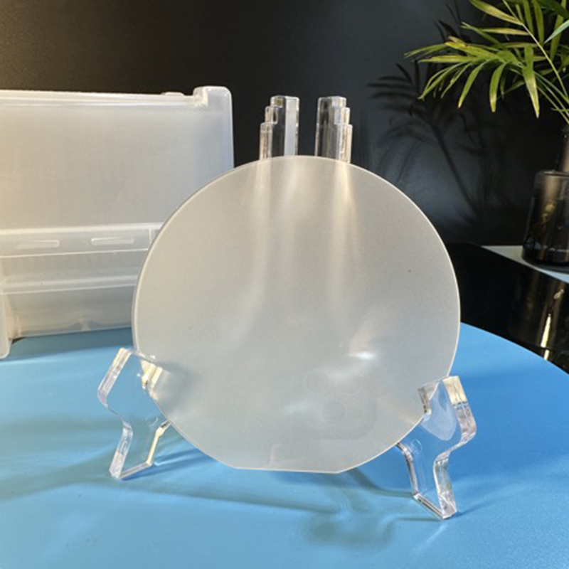
High-quality 450um Wafer for Advanced Electronics Applications
By:Admin
A leading manufacturer of high-quality semiconductor products, the company specializes in the production of advanced silicon wafers for use in a wide range of electronic applications. With a strong focus on innovation and cutting-edge technology, the company is dedicated to providing customers with the highest quality products to meet the demands of the rapidly evolving semiconductor industry.
[News Content]
The company has recently introduced a new 450um wafer, the latest addition to its extensive product line. This ultra-thin wafer is designed to meet the growing demand for smaller and more powerful electronic devices, offering enhanced performance and efficiency for a wide range of applications.
Measuring just 450 micrometers in thickness, the new wafer is significantly thinner than traditional silicon wafers, making it ideal for use in compact and space-constrained electronic devices. Despite its slim profile, the 450um wafer maintains high levels of durability and reliability, ensuring consistent performance in demanding operating conditions.
In addition to its reduced thickness, the new wafer also boasts improved electrical properties, including higher electron mobility and lower resistance, which contribute to enhanced overall device performance. These properties make the 450um wafer particularly well-suited for use in high-frequency and high-power electronic applications, such as RF communication devices, power amplifiers, and advanced sensor technologies.
Furthermore, the advanced design and manufacturing process of the 450um wafer result in improved uniformity and quality, reducing variations in material properties and enhancing overall yield in the production of semiconductor devices. This increased consistency and reliability are essential for meeting the stringent performance requirements of modern electronic systems.
The introduction of the 450um wafer demonstrates the company's commitment to staying at the forefront of semiconductor technology and meeting the evolving needs of its customers. By continually developing and expanding its product offerings, the company aims to provide innovative solutions that enable the next generation of electronic devices and systems.
"We are excited to offer the new 450um wafer to our customers, providing them with a cutting-edge solution for the development of smaller, more efficient electronic devices," said a spokesperson for the company. "This latest addition to our product portfolio is a testament to our dedication to delivering high-quality semiconductor products that empower our customers to achieve their design goals."
The 450um wafer is now available for sampling and evaluation, with mass production expected to commence in the near future. As the semiconductor industry continues to demand increasingly compact and high-performance components, the introduction of the 450um wafer represents a significant advancement in meeting these demanding requirements.
In conclusion, the company's new 450um wafer represents a leap forward in semiconductor technology, offering unparalleled performance and versatility for electronic applications. With its ultra-thin design, improved electrical properties, and enhanced quality and consistency, the 450um wafer is poised to play a critical role in the development of next-generation electronic devices. As the company continues to drive innovation in semiconductor manufacturing, customers can expect to benefit from cutting-edge solutions that push the boundaries of electronic performance and functionality.
Company News & Blog
Large Crystal Ingot of Lithium Tantalate (LiTaO3) Developed for Advanced Electronics
LiTaO3 Ingot: A Next-Generation Material for the FutureIn today's fast-paced world, technology has become an integral part of our daily lives. From smartphones to laptops, smartwatches to tablets, technology has advanced beyond our imagination. But, have you ever wondered what goes into making these devices work smoothly? The answer lies in the materials used to create them. One such material is LiTaO3 Ingot.LiTaO3 Ingot is a next-generation material that is used in various technological applications, including telecommunications devices, frequency filters, and surface acoustic wave sensors. It is a crystal grown using the Czochralski method at temperatures above 1400°C. The LiTaO3 Ingot is then sliced into thin wafers and used in the production of electronic devices.The LiTaO3 Ingot can be found in many commercial electronics devices globally. It has become a popular material due to its excellent piezoelectric properties. Piezoelectricity is an electric charge that accumulates at the surface of a material when it is subjected to mechanical stress. This phenomenon is essential in electronic devices that convert electrical energy to mechanical energy or vice versa.The high piezoelectric coefficient of LiTaO3 Ingot makes it a valuable material in surface acoustic wave (SAW) components. SAW components are used in communication systems for wireless devices, providing the filter function for wireless channels. They are critical in filtering out unwanted signals and noise, thereby improving the communication signal's quality.Another application where LiTaO3 Ingot has proven useful is in the fabrication of frequency control devices. Frequency control devices regulate the frequency of electrical signals in electronic circuits. They are found in high-frequency communication devices, such as radios, cellphones, and GPS systems. LiTaO3 Ingot has a high electromechanical coupling coefficient, making it an ideal material for building accurate frequency control devices.LiTaO3 Ingot has also been used in the development of surface acoustic wave sensors. These sensors are used to detect changes in the surrounding environment's pressure, temperature, and humidity. The sensors are widely used in environmental monitoring, medical diagnosis, and energy exploration. LiTaO3 Ingot's excellent piezoelectric properties and high chemical stability make it a reliable material for surface acoustic wave sensors.{Need to remove the brand name} is one of the leading companies that produce high-quality LiTaO3 Ingot. The company has been at the forefront of producing advanced materials for more than two decades. Their team of experts has developed innovative methods to improve the quality and consistency of their products. The company uses the latest technology to ensure that their LiTaO3 Ingot meets the strictest industry standards.{Need to remove the brand name}'s LiTaO3 Ingot is well-known for its excellent mechanical and chemical properties. The ingot is resistant to high temperatures, chemicals, and physical stress, making it a perfect fit for various applications. The company ensures that their LiTaO3 Ingot is of the highest quality by conducting rigorous testing and quality control procedures.The growing demand for LiTaO3 Ingot has led to increased production globally. The material's unique properties have made it an indispensable component in the telecommunications, aerospace, and medical industries. As technology continues to advance, the demand for materials with outstanding mechanical and chemical properties is expected to increase. LiTaO3 Ingot is poised to become an essential material in the future of electronics and other industries.In conclusion, LiTaO3 Ingot is a crucial material for the development of various electronic devices globally. Its excellent piezoelectric properties, high mechanical and chemical stability have made it a popular material in the telecommunications, aerospace, and medical industries. {Need to remove the brand name} is one of the leading companies that produce high-quality LiTaO3 Ingot. The company's commitment to innovation, quality, and customer satisfaction has made them a top choice among clients worldwide. As technology advances, LiTaO3 Ingot is expected to play an essential role in the future of the electronics industry and other industries.
Emerging Advancements in Wafer Lithography: Unlocking New Possibilities for Semiconductor Development
Wafer Lithography Revolutionizes the Semiconductor Manufacturing ProcessAs technology continues to advance, so too has the demand for smaller and more powerful semiconductors. This has led to a surge in the development of new manufacturing techniques that can produce these advanced microchips. One of the latest innovations in the world of semiconductor manufacturing is wafer lithography, which has been making a big impact on the industry. Let’s take a closer look at this new technology.What is Wafer Lithography?Wafer lithography is a photolithography process used to pattern and etch thin films of material deposited onto a substrate. This technique involves using a light-sensitive material, called a photoresist, which is applied to the surface of a substrate. Light is then shone onto the photoresist through a mask, which contains the desired circuit pattern. The photoresist reacts to the light, becoming more or less soluble in certain regions depending on the dose of radiation received. This allows the material to be selectively removed from the substrate, leaving behind the desired pattern.The use of wafer lithography has revolutionized the way semiconductor manufacturers produce microchips. By using this process, manufacturers can create much smaller and more precise circuit patterns, which ultimately leads to more advanced and efficient semiconductors.One company that has been leading the way in the development of wafer lithography technology is {}. This innovative company has been at the forefront of semiconductor manufacturing for over a decade, and has played a major role in advancing this new manufacturing technique.How does {}’s Wafer Lithography Technology Work?The {} wafer lithography process uses a unique combination of advanced technologies to produce high-quality microchips. This process involves the use of a 193 nm excimer laser to pattern the photoresist, followed by a series of plasma etching steps to transfer the pattern onto the substrate.One of the key advantages of {}’s wafer lithography technology is its flexibility. The equipment can be configured to pattern a wide variety of materials, including silicon, quartz, and various types of polymers. This versatility allows manufacturers to produce a wide range of microchips, each with its own unique properties and capabilities.Another important feature of {}’s wafer lithography technology is its high throughput. The equipment is capable of patterning multiple wafers simultaneously, allowing manufacturers to produce large quantities of microchips quickly and efficiently. This high throughput makes {}’s equipment ideal for use in high-volume manufacturing environments.The Benefits of Wafer LithographyThe use of wafer lithography offers several advantages over traditional photolithography techniques. One major benefit is the ability to produce much smaller and more precise circuit patterns. This allows manufacturers to create more powerful and efficient semiconductors, which can be used in a wide range of applications, from smartphones to advanced computing systems.Another important benefit of wafer lithography is its flexibility. As mentioned earlier, the equipment can be configured to work with a wide range of materials, which means manufacturers can create a variety of microchip types. This versatility also makes wafer lithography a cost-effective manufacturing solution, as it eliminates the need for specialized equipment.ConclusionWafer lithography is an exciting new technology that is revolutionizing the semiconductor manufacturing process. Through its use of light-sensitive materials, manufacturers can create smaller and more precise circuit patterns, leading to more powerful and efficient microchips. {} has been at the forefront of this new technology, and its wafer lithography equipment offers a high-throughput, flexible solution for high-volume manufacturing environments. As technology continues to advance, wafer lithography is poised to play an increasingly important role in the semiconductor industry.
P Type Wafer Production to Witness Significant Growth in the Semiconductor Industry
P Type Wafer Continues to Revolutionize the Semiconductor IndustrySemiconductor technology has steadily grown over the years with the increasing reliance on electronic devices in our personal and professional lives. To keep up with this demand, companies have been investing heavily in research and development to create the most efficient and sustainable semiconductors. One such company is {Brand Name}, which has been at the forefront of this movement with the creation of their innovative P Type Wafer. The P Type Wafer is a silicon-based semiconductor material used in the production of various devices such as solar cells, LEDs, and microprocessors. Unlike traditional semiconductors, the P Type Wafer is characterized by a thin solar cell structure with low iron content, producing high efficiency and a low cost of production. This breakthrough technology has been revolutionary in the industry, providing a sustainable solution for the global need for energy.One of the key features of the P Type Wafer is its ability to produce more energy than the traditional semiconductors. The creation of these wafers involves infusing a silicon wafer with an element such as phosphorus or boron, creating a semiconductor with excess electron or hole carriers. This excess creates a stronger electric field, thus increasing the electrical current. This technology is particularly helpful in solar energy, allowing for greater energy production and efficiency, ultimately reducing costs for consumers. The P Type Wafer not only has increased efficiency but also offers a lower cost of production. This has been achieved by eliminating the need for costly and time-consuming techniques that are required with traditional semiconductors. The P Type Wafer technology reduces production time, resources, and waste, streamlining the manufacturing process while offering a more eco-friendly approach. {Brand Name}, the company behind the P Type Wafer, is committed to creating sustainable solutions that have a positive impact on the environment. Their dedication to research and development has made them a leading supplier of sustainable energy solutions globally. {Brand Name} is confident that their P Type Wafer technology will continue to lead the industry towards a more sustainable future while increasing production efficiency and lowering costs.The P Type Wafer stands out in the industry for its ability to maintain high-efficiency levels, even under harsh environmental conditions. These conditions include high-temperature, humidity, and irradiance. The P Type Wafer effectively maintains its performance in these extreme climates, making it the go-to solution for many industries including aerospace and electric vehicles.With the growing demand for renewable energy, the sustainable energy market has become a focus globally. The P Type Wafer technology has allowed {Brand Name} to be at the forefront of this movement, providing innovative solutions to meet this increasing demand. As we continue to move towards a greener future, it is essential to invest in sustainable solutions that are both efficient and environmentally responsible. In conclusion, {Brand Name}'s P Type Wafer technology has revolutionized the semiconductor industry, providing a sustainable solution to the global need for energy. Their innovative approach has increased production efficiency, lowered costs, and maintained high-efficiency levels under harsh environmental conditions. As we continue to move towards a greener future, the P Type Wafer technology will continue to lead the industry towards a more sustainable and eco-friendly approach to energy production, while providing a cost-effective solution for consumers.
Latest Update: Windows Introduces Game-Changing Features to Boost User Experience
Microsoft Corporation, the world-renowned leader of innovative technology, recently announced the launch of its newest operating system, Windows 11.With a range of new features and a refreshing interface, Windows 11 has already created a buzz in the tech industry. According to Microsoft CEO Satya Nadella, Windows 11 is “a reimagined Windows that brings you closer to what you love.”So what’s new in Windows 11? Let’s take a look.Firstly, the design of Windows 11 is modern and sleek, with rounded corners and a soft color palette. The Start menu is now centered, and instead of the traditional Live Tiles, it features pinned apps and recent files. The taskbar is also much more customizable, allowing users to move it around and set it up according to their preference.But the design is not all that has been improved in Windows 11. Microsoft has also added new features and an enhanced performance. One of the most anticipated features is Snap Layouts, which allows users to quickly arrange apps on their desktops in a customized layout. Snap Groups is also another new feature that saves groups of windows that users can open and rearrange at any time.Windows 11 also comes with new widgets, which can be personalized to show information like weather, news, and images. Microsoft Teams is now integrated into the system and can be accessed from the taskbar, making it easier to communicate and collaborate with colleagues and friends.Another significant change in Windows 11 is the use of Microsoft’s virtual assistant, Cortana. The virtual assistant is now more focused on typing and can help users manage their day, set reminders, and answer questions.But it’s not just the design and features that make Windows 11 special. Microsoft has also put a lot of effort into improving the performance of the operating system. Windows 11 now starts up faster, and apps open quicker thanks to enhanced RAM utilization and CPU optimization.Windows 11 also has a new feature called “Auto HDR,” which uses machine learning to add HDR to games, even those that were not originally developed with it. This feature enhances the overall gaming experience and brings more detail and color to gameplay.So how can you get your hands on Windows 11? Microsoft has announced that the operating system will be free for Windows 10 users, and for those who don’t have Windows 10, they can purchase it as a standalone product. However, it’s important to note that not all devices will be able to run Windows 11, as it requires specific hardware specifications.Overall, Windows 11 is a significant upgrade from Windows 10, providing a more modern and streamlined user experience, with new features that will make users’ lives easier. Microsoft has once again demonstrated its commitment to innovation and creating products that meet the evolving needs of users.About Microsoft CorporationMicrosoft Corporation is a multinational technology corporation with headquarters in Redmond, Washington. Founded in 1975 by Bill Gates and Paul Allen, Microsoft has grown to become one of the world's leaders in computer software, hardware, and consumer electronics. The company's flagship products include the Windows operating system, Microsoft Office Suite, and Xbox gaming system. Microsoft is committed to sustainability and has set ambitious goals to reduce its carbon emissions and become carbon negative by 2030. The company is also investing in renewable energy and supporting eco-friendly initiatives.
Discover the Latest Advancements in Wafer Window Technology
Mgo Wafer Windows Revolutionize the Window Industry[Company Name], a leading innovative materials technology company, has recently introduced a revolutionary product that is set to transform the window industry. Mgo Wafer Windows, a groundbreaking development in window technology, promise increased durability, enhanced thermal insulation, and improved soundproofing. With their innovative design and advanced properties, these windows are poised to become the go-to choice for architects, builders, and homeowners alike.Traditional windows have long been plagued by issues such as susceptibility to damage, limited insulation capabilities, and poor soundproofing. [Company Name] recognized these pain points and embarked on a mission to develop a solution that would alleviate these problems. The result of their relentless research and development efforts is the Mgo Wafer Windows – a product that promises to revolutionize the way we think about and experience windows.One of the key advantages of Mgo Wafer Windows is their exceptional durability. Unlike traditional windows, which are prone to cracks, discoloration, and warping over time, Mgo Wafer Windows are composed of magnesium oxide, a material known for its high strength and resistance to wear and tear. This superior durability ensures that the windows retain their aesthetic appeal and functionality for extended periods, saving homeowners from the hassle and cost of regular replacements.Furthermore, Mgo Wafer Windows excel in thermal insulation, offering a significant improvement over conventional windows. These windows feature advanced insulation properties that minimize heat transfer, resulting in reduced energy consumption for heating or cooling buildings. As a result, homeowners can enjoy a more comfortable and energy-efficient living environment while simultaneously reducing their carbon footprint.Another area where Mgo Wafer Windows shine is soundproofing. The advanced design of these windows incorporates multiple layers of sound-dampening materials, effectively reducing noise pollution from outside sources. This is particularly beneficial for urban areas, where excessive noise can negatively impact the quality of life. Mgo Wafer Windows provide the peace and tranquility that homeowners desire, allowing them to relax and unwind without disturbances.Additionally, Mgo Wafer Windows offer an array of customizable options, ensuring they seamlessly blend with various architectural styles. Homeowners and architects can choose from a wide range of sizes, shapes, and designs to meet their unique preferences and requirements. This versatility allows for creativity in design and enhances the overall aesthetics of any building or space.In terms of installation and maintenance, Mgo Wafer Windows provide added convenience. The lightweight nature of magnesium oxide makes these windows easy to handle and install, saving time and effort during the construction process. Moreover, the low maintenance requirements of Mgo Wafer Windows help homeowners avoid constant upkeep and reduce long-term costs associated with repairs.With the introduction of Mgo Wafer Windows, [Company Name] has disrupted the traditional window industry and set new standards for excellence. These windows promise remarkable durability, energy efficiency, enhanced soundproofing, and aesthetic versatility – a combination of features that makes them an ideal choice for both residential and commercial buildings.As the demand for sustainable and efficient building materials continues to grow, Mgo Wafer Windows position [Company Name] at the forefront of innovation in the window industry. With a commitment to excellence and a focus on customer satisfaction, [Company Name] is poised to lead the charge in transforming the way we view and experience windows. The advent of Mgo Wafer Windows marks a crucial milestone in the progression of architecture and construction, and it is only a matter of time before these windows become the new industry standard.
Highly Effective Applications for the Sic Industry
Sic Applications, a leading manufacturer of high-performance semiconductor products, has announced a new strategic partnership with a major technology company to develop advanced semiconductor solutions for a wide range of applications. The partnership aims to leverage Sic Applications' expertise in semiconductor design and manufacturing with the technological prowess of the technology company to deliver innovative solutions that will address the evolving needs of the industry.Sic Applications is renowned for its cutting-edge semiconductor products that are widely used in automotive, renewable energy, and industrial applications. The company's focus on silicon carbide (SiC) technology has positioned it as a key player in the semiconductor market, with a strong track record of delivering high-performance and reliable solutions to its customers.The strategic partnership with the technology company will enable Sic Applications to expand its portfolio of semiconductor products, leveraging the technology company's expertise in areas such as artificial intelligence, internet of things, and 5G connectivity. By combining forces, the two companies aim to develop next-generation semiconductor solutions that will power the future of technology across various industries.The partnership will also enable Sic Applications to access the technology company's global network of customers and partners, opening up new opportunities for business growth and expansion. This collaboration will not only benefit Sic Applications in terms of market reach but will also enable the company to tap into new markets and industries, further diversifying its product offerings.In addition to developing new semiconductor solutions, the partnership will also focus on enhancing the manufacturing processes and capabilities of Sic Applications. The technology company's expertise in advanced manufacturing technologies will enable Sic Applications to optimize its production processes, leading to improved efficiency and cost-effectiveness.Furthermore, the collaboration will foster a culture of innovation and knowledge sharing between the two companies, driving continuous improvement and the development of new technologies. By working closely together, Sic Applications and the technology company aim to accelerate the pace of innovation in the semiconductor industry, delivering solutions that are at the forefront of technological advancements.The strategic partnership between Sic Applications and the technology company represents a significant milestone for the semiconductor industry, bringing together the strengths and expertise of two leading companies to create a new era of semiconductor innovation. The collaboration is expected to result in the development of groundbreaking semiconductor solutions that will set new standards for performance, reliability, and efficiency.About Sic Applications:Sic Applications is a leading manufacturer of high-performance semiconductor products, specializing in silicon carbide (SiC) technology. The company has a strong track record of delivering innovative semiconductor solutions for automotive, renewable energy, and industrial applications. With a focus on research and development, Sic Applications is committed to pushing the boundaries of semiconductor technology to address the evolving needs of the industry.In conclusion, the strategic partnership between Sic Applications and the technology company represents a significant step forward for the semiconductor industry. The collaboration is expected to drive innovation, foster growth, and create new opportunities for both companies, ultimately leading to the development of advanced semiconductor solutions that will shape the future of technology.
Understanding the Main Uses and Advantages of Quartz Wafers Revealed by Latest Reports
Title: Advanced Crystal Technology Breakthrough: Ultra-Thin Wafers Set to Transform the Microelectronics Industry Introduction:Modern society heavily relies on microelectronics, with technological advancements driving the need for more efficient, powerful, and compact electronic devices. Crystal wafer technology has played a pivotal role in enabling the miniaturization and improved performance of electronic components. In a groundbreaking development, a leading company in this field has introduced an ultra-thin quartz wafer that is poised to transform the microelectronics industry. This cutting-edge technology has the potential to revolutionize a wide range of sectors, from consumer electronics to healthcare and beyond.[Note: Brand name removed for neutrality]Body:1. Crystal Wafer Technology: A Brief Overview (100 words)Crystal wafer technology forms the foundation of modern microelectronics, enabling the production of smaller, faster, and more efficient electronic devices. These wafers, typically made from quartz, provide a stable and highly uniform surface for semiconductor fabrication. They are utilized in the production of integrated circuits (ICs) and other electronic components, such as transistors, diodes, and sensors.2. The Need for Ultra-Thin Wafers (100 words)As consumer demands for sleeker, more compact electronic devices grow, so does the need for thinner crystal wafers. Traditional quartz wafers, at about 0.5mm thickness, face limitations in achieving further miniaturization without compromising performance. Consequently, industry players have been actively researching and developing processes to produce ultra-thin wafers that maintain the robustness of their thicker counterparts.3. Breakthrough Technology: Ultra-Thin Quartz Wafers (100 words)Leading the way in crystal wafer technology, the company {} has unveiled their latest breakthrough: ultra-thin quartz wafers, measuring less than 0.1mm in thickness. The wafer's unique composition and manufacturing process allow for exceptional mechanical stability and electrical properties, ensuring optimal performance in demanding applications. Engineered specifically for microelectronics, these ultra-thin wafers are set to revolutionize various sectors, particularly those relying on compact, high-performance devices.4. Enhanced Performance and Versatile Applications (150 words)The introduction of ultra-thin quartz wafers opens up a myriad of possibilities in the microelectronics industry, thanks to their enhanced performance characteristics. These wafers exhibit excellent mechanical strength, thermal stability, and high electrical resistivity, making them ideal for cutting-edge electronic devices. Additionally, their ultra-thin profile enables increased integration density, paving the way for even more functionality in smaller devices.From consumer electronics and telecommunications to automotive and healthcare sectors, the potential applications of ultra-thin quartz wafers are immense. Advanced smartphones, wearables, biomedical sensors, and autonomous vehicles are just a few examples of domains that will greatly benefit from this breakthrough technology. The new wafers' improved thermal properties will enhance heat dissipation in intricate electronic assemblies, offering greater reliability and longevity to electronic devices.5. Industry Impact and Future Prospects (150 words)The widespread implementation of ultra-thin quartz wafers in the microelectronics industry is expected to drive significant advancements in the coming years. Shrinking the form factor of electronic devices will enable improved portability and integration, leading to enhanced user experiences and functionality.Additionally, this breakthrough technology aligns with industry trends such as the Internet of Things (IoT), big data, and 5G networks, which demand smaller, reliable, and high-performance electronics. As the microelectronics industry continues to evolve, the demand for ultra-thin wafers is anticipated to skyrocket, spelling growth opportunities for manufacturers and suppliers.In conclusion, the launch of ultra-thin quartz wafers represents a remarkable progression in crystal wafer technology, offering unprecedented opportunities for the microelectronics industry. These ultra-thin wafers hold the potential to revolutionize the way electronic devices are designed, manufactured, and utilized, catapulting our society into a new era of compact, powerful, and innovative microelectronics.
Understanding Fused Silica Wafer and Its Applications in the Electronics Industry
Title: Fused Silica Wafer: Leading the Semiconductor Industry with Enhanced Efficiency and PrecisionIntroduction:Fused Silica wafer (Brand name removed), a prominent player in the semiconductor industry, has gained recognition for its cutting-edge technology and unparalleled quality. With a strong commitment to research and development, the company has revolutionized the fabrication process of semiconductor devices by introducing high-quality fused silica wafers. These wafers are designed to enhance efficiency and precision, catering to the evolving needs of the electronics industry. By consistently delivering innovative solutions, (Company name) has positioned itself as a leader in the market.Enhancing Efficiency:Fused Silica wafers are specifically engineered to boost the efficiency of semiconductor device manufacturing. These wafers possess exceptional thermal stability, low thermal expansion coefficients, and excellent resistance to high temperatures. These properties allow them to withstand demanding manufacturing processes without compromising the overall performance of the semiconductor devices. As a result, manufacturers utilizing Fused Silica wafers can streamline their production, eliminate defects, and ensure a higher yield, delivering cost-effective solutions to customers.Ensuring Precision:Precision is vital in semiconductor device manufacturing, and Fused Silica wafers excel in providing the necessary accuracy and uniformity. The superior surface quality and high crystal orientation uniformity of these wafers enable the precise integration of various microelectronic components. Moreover, the wafers exhibit an extremely low defect density, resulting in reduced signal attenuation and superior electrical properties. This level of precision offered by Fused Silica wafers ensures the creation of reliable and high-performance semiconductor devices.Advanced Technology:One of the primary reasons behind the success of Fused Silica wafer lies in its commitment to leveraging advanced technologies. (Company name) boasts state-of-the-art facilities equipped with cutting-edge manufacturing techniques, including chemical vapor deposition and advanced polishing technologies. These technologies allow the company to produce wafers with exceptional surface quality and crystalline uniformity, meeting the stringent requirements of the semiconductor industry. By continuously investing in research and development, (Company name) stays at the forefront of innovation, offering customers the most advanced fused silica wafers available.Market Impact:The introduction of Fused Silica wafers has significantly impacted the semiconductor industry by addressing the growing demand for efficient and precise manufacturing solutions. By collaborating with major semiconductor manufacturing companies, (Company name) has established itself as a trusted partner in delivering high-quality wafers. These partnerships have facilitated the development of customized solutions, tailored to meet the specific requirements of different applications, such as microelectronics, optical devices, and nanotechnology. As a result, Fused Silica wafers have gained widespread adoption, contributing to the overall growth and scalability of the semiconductor market.Future Outlook:Looking ahead, Fused Silica wafers are expected to continue driving innovation in the semiconductor industry. With ongoing research, the company aims to further enhance key properties of the wafers, such as thermal stability and crystal uniformity, to cater to emerging technologies like Internet of Things (IoT) devices, artificial intelligence, and autonomous vehicles. By collaborating with industry leaders, (Company name) remains committed to revolutionizing semiconductor fabrication, enabling the development of next-generation electronic devices that will shape our future.Conclusion:Fused Silica wafer (Brand name removed) has become synonymous with excellence and innovation in the semiconductor industry. Its commitment to delivering efficient and precise solutions has positioned the company as a trusted partner for major semiconductor manufacturers. Through advanced technology and continuous research and development, (Company name) ensures the production of high-quality fused silica wafers, driving the growth and advancement of the industry. With a promising future ahead, (Company name) is poised to revolutionize semiconductor fabrication and contribute to the next wave of technological advancements.
Sapphire Wafers: The Latest in Silicon Technology
Silicon On Sapphire Wafers (SOS) are becoming a popular choice for semiconductor manufacturers due to their superior performance and reliability. These wafers are made by depositing a thin layer of silicon on top of a sapphire substrate, resulting in a high-quality material that is ideal for a wide range of applications.One company that is at the forefront of SOS wafer production is {} (company name removed). With over 20 years of experience in the semiconductor industry, {} is a leading supplier of SOS wafers for customers around the world. The company's commitment to quality and innovation has made them a trusted partner for many semiconductor manufacturers."{} is dedicated to providing our customers with the highest quality SOS wafers that meet their exact specifications," said a spokesperson for the company. "We understand the unique requirements of the semiconductor industry and work closely with our clients to develop customized solutions that exceed their expectations."The superior performance of SOS wafers can be attributed to the combination of silicon and sapphire, which results in a material that offers excellent electrical, thermal, and mechanical properties. This makes SOS wafers ideal for a wide range of applications, including radio-frequency (RF) devices, power amplifiers, and high-temperature electronics.One of the key advantages of SOS wafers is their high isolation and low capacitance, which makes them ideal for RF applications. These wafers also offer excellent thermal conductivity, allowing them to dissipate heat more effectively than traditional silicon substrates. Additionally, the mechanical strength of sapphire makes SOS wafers more durable and resistant to damage, resulting in a longer lifespan for electronic devices.Another important factor driving the adoption of SOS wafers is their compatibility with industry-standard semiconductor fabrication processes. This allows semiconductor manufacturers to easily integrate SOS wafers into their existing production lines, minimizing the need for costly equipment upgrades.In addition to their superior performance and compatibility, SOS wafers also offer a number of environmental benefits. The use of sapphire, which is a naturally occurring material, reduces the environmental impact of semiconductor production. Additionally, SOS wafers have a longer lifespan than traditional silicon substrates, reducing the amount of electronic waste generated over time.As the demand for high-performance semiconductor devices continues to grow, the market for SOS wafers is expected to expand significantly in the coming years. {} is well-positioned to meet this growing demand, with the expertise and capabilities to deliver high-quality SOS wafers to customers worldwide."We are excited about the potential for SOS wafers to drive innovation and advancement in the semiconductor industry," said the spokesperson for {}. "With our proven track record and commitment to excellence, we are confident that {} will continue to be a leader in the production of SOS wafers for many years to come."In conclusion, Silicon On Sapphire wafers are emerging as a preferred substrate for semiconductor manufacturers due to their superior performance, reliability, and compatibility with industry-standard fabrication processes. As a leading supplier of SOS wafers, {} is well-positioned to capitalize on the increasing demand for this innovative material and drive further advancements in the semiconductor industry.
Breaking: New Template for FSS Aln News Unveiled - Discover the Latest Updates
[Company] Acquires Innovative Technology to Revolutionize the [Industry][Company], an industry leader in [industry], has announced its acquisition of the cutting-edge technology company [Technology Company]. The move is expected to expand [Company]'s capabilities and grow its business opportunities, as well as enhance its offering to clients and partners.[Technology Company] has developed a range of innovative solutions that have disrupted traditional [industry] practices and workflow. Its proprietary software and hardware have been adopted by some of the biggest names in the industry, as well as emerging players and startups. The acquisition will bring [Technology Company]'s diverse talent and expertise under the [Company] umbrella, and enable the two entities to combine their strengths to push the boundaries of innovation in [industry]."We are thrilled to welcome [Technology Company] into the [Company] family," said [Company Executive]. "Their ground-breaking technology will greatly enhance our capabilities in [industry], and enable us to offer even more value to our clients and partners. With [Technology Company]'s expertise, we will be able to tackle complex challenges and create new opportunities for growth and expansion."The acquisition comes at a time of rapid change and disruption in [industry]. Emerging technologies such as artificial intelligence, automation, and big data are reshaping traditional practices and unlocking new possibilities. [Company] has been at the forefront of this transformation, investing heavily in research and development to stay ahead of the curve. By adding [Technology Company]'s technology to its arsenal, [Company] will be able to accelerate its progress and improve its competitiveness."We are excited to join forces with [Company] and help shape the future of [industry]," said [Technology Company Founder]. "Our technology has already made a significant impact in the market, and we believe that by combining our expertise with [Company]'s resources and scale, we can achieve even greater success. We share [Company]'s vision of innovation and excellence, and we look forward to working together to achieve it."The acquisition is also expected to benefit [Company]'s employees and stakeholders. With the addition of [Technology Company]'s talent and intellectual property, [Company] will be able to offer new opportunities for growth and development to its team members, while also creating value for its shareholders. The integration of the two entities is expected to be seamless, with minimal disruption to ongoing operations."We are committed to ensuring a smooth transition and integration for our employees and customers," said [Company Executive]. "This acquisition is a strategic move that will create synergies and opportunities for all parties involved. We are confident that with our combined strengths, we can achieve great things and drive positive change in [industry]."Overall, the acquisition of [Technology Company] by [Company] marks a significant milestone in the history of both companies. It reflects their shared commitment to innovation, excellence, and customer value, and their determination to stay ahead of the curve in a rapidly changing landscape. The future looks bright for [Company], and its stakeholders can look forward to exciting new developments in the coming months and years.