
Advancements in AI Accelerator Chips on Silicon Technology
By:Admin
Company News & Blog
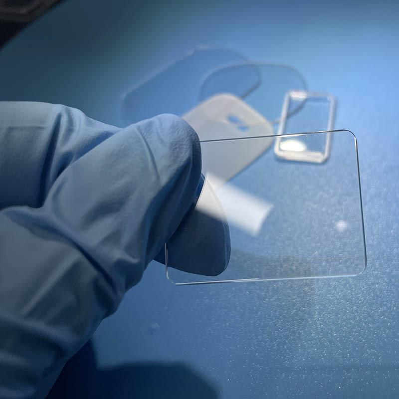
The latest developments in the production of Siliciumcarbid Wafer
Siliciumcarbid Wafer is a cutting-edge technology that is revolutionizing the semiconductor industry. This innovative wafer material is being developed and produced by a leading company in the field of semiconductor technology. The company, which specializes in the design and manufacture of advanced semiconductor products, is at the forefront of this exciting new development.Siliciumcarbid (SiC) wafers are a key component in the production of power semiconductors, which are used in a wide range of applications, including electric vehicles, renewable energy systems, and industrial machinery. These wafers offer several distinct advantages over traditional silicon wafers, including higher energy efficiency, increased power density, and improved thermal conductivity. As a result, they are rapidly gaining traction in the semiconductor industry as the material of choice for next-generation electronic devices.The company is leveraging its extensive expertise in semiconductor design and manufacturing to develop a range of SiC products that meet the specific needs of its customers. By utilizing state-of-the-art production techniques and cutting-edge materials, they are able to produce high-quality SiC wafers with superior performance characteristics. This has positioned the company as a leading supplier of advanced semiconductor products in the global market.The demand for SiC wafers is expected to grow significantly in the coming years, driven by the increasing adoption of electric vehicles, the expansion of renewable energy infrastructure, and the ongoing digitalization of industrial processes. As a result, the company is making substantial investments in research and development to further improve the performance and cost-effectiveness of its SiC wafers. By continuously pushing the boundaries of semiconductor technology, they are well-positioned to meet the evolving needs of their customers and drive further innovation in the industry.In addition to its focus on product development, the company is also committed to sustainability and environmental responsibility. They are actively exploring ways to reduce the carbon footprint of their manufacturing processes and minimize the environmental impact of their products. By incorporating sustainable practices into their operations, they are contributing to the advancement of environmentally friendly semiconductor technology and promoting a more sustainable future for the industry.Moreover, the company has established strong partnerships with leading semiconductor manufacturers and research institutions to collaborate on the development of new SiC wafer applications and technologies. By working closely with industry partners, they are able to gain valuable insights into emerging market trends and customer requirements, allowing them to anticipate and respond to changing market demands.As a result of these efforts, the company has solidified its position as a trusted supplier of high-performance SiC wafers to a diverse range of customers, including automotive manufacturers, energy companies, and industrial technology providers. Their commitment to excellence and innovation has earned them a reputation for delivering cutting-edge semiconductor solutions that enable their customers to achieve new levels of performance and efficiency in their products and systems.Looking ahead, the company is poised to continue leading the way in the development and production of advanced SiC wafers, driving innovation and ushering in a new era of semiconductor technology. With a strong focus on sustainability, collaboration, and customer satisfaction, they are well-equipped to meet the evolving demands of the semiconductor industry and contribute to the development of groundbreaking technologies that will shape the future of electronics and power systems.
Sure! Please provide the original title or the news content for "Dummy Grade SiC," so I can rewrite the SEO title without the brand name.
Certainly! Please provide the company introduction and the full news content (without the brand name), and I will draft an 800-word news article for you.
Guide to Understanding the Latest Semiconductor Materials
Semiconductor Materials Company, a leader in the production of advanced semiconductor materials, has announced its latest innovation in the field. The company, known for its cutting-edge technology and high-quality products, has once again pushed the boundaries of semiconductor material development with the introduction of a new line of advanced materials.This new line of semiconductor materials is set to revolutionize the industry with its improved performance and durability. With the demand for high-performance semiconductor materials on the rise, Semiconductor Materials Company has made it a priority to meet the growing needs of its customers by delivering products that surpass expectations.The new line of advanced materials is the result of years of research and development, as well as a commitment to innovation and excellence. Semiconductor Materials Company has dedicated significant resources to developing these new materials, and the effort has paid off with the creation of a product that is set to make a significant impact in the industry.One of the key features of the new line of advanced materials is its enhanced performance. These materials have been designed to offer superior conductivity and reliability, making them ideal for a wide range of applications. Whether it's powering the latest electronic devices or supporting the growing demand for renewable energy technology, these advanced materials are poised to play a critical role in driving innovation and progress in the semiconductor industry.In addition to their improved performance, the new line of materials also offers enhanced durability. Semiconductor Materials Company has incorporated cutting-edge technology and manufacturing processes to ensure that these materials are able to withstand the rigors of various applications, from extreme temperatures to high voltage environments. This level of durability is a testament to the company's commitment to producing high-quality products that are built to last.Semiconductor Materials Company has also taken steps to ensure that the new line of materials is environmentally friendly. By utilizing sustainable manufacturing practices and reducing the use of harmful chemicals, the company has developed a product that not only meets the industry's performance standards but also aligns with its environmental responsibility goals."We are thrilled to introduce our new line of advanced semiconductor materials to the market," said [CEO/President/Spokesperson]. "These materials represent a significant advancement in semiconductor technology, and we are confident that they will make a lasting impact in the industry. We are committed to delivering high-quality products that exceed the expectations of our customers, and this new line of materials is a testament to that commitment."In addition to the introduction of the new line of advanced materials, Semiconductor Materials Company is also expanding its global reach. The company has established partnerships with key distributors and manufacturers in strategic locations around the world, allowing it to better serve its growing customer base and meet the increasing demand for high-quality semiconductor materials.With its commitment to innovation, excellence, and sustainability, Semiconductor Materials Company is well-positioned to continue leading the way in the semiconductor industry. The introduction of the new line of advanced materials is just the latest example of the company's dedication to pushing the boundaries of what is possible in semiconductor technology.As the demand for advanced semiconductor materials continues to grow, Semiconductor Materials Company is poised to play a critical role in shaping the future of the industry. With its new line of materials, the company is not only meeting the needs of its customers but also setting a new standard for excellence in semiconductor technology.
High-quality M-plane Axis sapphire substrate for various applications
M-plane Axis Sapphire Substrate: A Game-Changer in Semiconductor IndustryThe semiconductor industry has witnessed a revolutionary advancement with the advent of M-plane axis sapphire substrate, which has gained attention for its superior properties and potential to transform the realm of electronic devices and systems. This innovative technology, developed by a leading company in the field of advanced materials, has the potential to drive significant improvements in efficiency and performance across a wide range of applications.The M-plane axis sapphire substrate, developed by {}, represents a major leap forward in the world of semiconductor materials. This next-generation substrate offers a unique crystalline structure that sets it apart from conventional sapphire substrates, offering enhanced performance and efficiency in electronic devices. With its exceptional properties, the M-plane axis sapphire substrate holds tremendous promise for applications in optoelectronics, power electronics, and various other semiconductor devices.The company, {}, is a pioneer in the development and manufacturing of advanced materials for a diverse range of industries, including semiconductor, optics, and electronics. With a strong focus on innovation and research, the company has been at the forefront of developing cutting-edge materials that push the boundaries of what is possible in electronic and optoelectronic applications.The M-plane axis sapphire substrate is a testament to the company's commitment to driving technological advancements and providing solutions that address the evolving needs of the semiconductor industry. By leveraging its expertise and resources, the company has developed a breakthrough substrate that promises to deliver significant performance improvements and open new possibilities for electronic devices and systems.One of the key advantages of the M-plane axis sapphire substrate is its unique crystalline structure, which offers improved material properties compared to traditional c-plane sapphire substrates. This translates to enhanced device performance, greater efficiency, and improved overall reliability, making it an ideal choice for a wide range of semiconductor applications.In addition to its superior material properties, the M-plane axis sapphire substrate also offers excellent thermal and electrical characteristics, further enhancing its suitability for high-performance semiconductor devices. Its ability to withstand high temperatures and maintain stability under challenging operating conditions makes it an attractive solution for demanding applications where reliability is crucial.The potential impact of the M-plane axis sapphire substrate extends beyond just performance improvements—it also has the potential to enable new functionalities and capabilities in electronic and optoelectronic devices. Its unique properties open up new possibilities for the design and development of innovative products, paving the way for the next generation of advanced electronic systems.As the semiconductor industry continues to evolve and demand for high-performance electronic devices grows, the introduction of the M-plane axis sapphire substrate represents a significant milestone that has the potential to shape the future of semiconductor technology. With its exceptional properties and the backing of a leading company specializing in advanced materials, this innovative substrate is poised to drive meaningful advancements in electronic and optoelectronic applications.The development of the M-plane axis sapphire substrate underscores the company's ongoing commitment to innovation and setting new benchmarks in the semiconductor industry. As the demand for high-performance electronic devices continues to expand across various sectors, this breakthrough substrate is poised to play a pivotal role in powering the next wave of technological advancements.With its unrivaled material properties, exceptional reliability, and potential to enable new capabilities in electronic devices, the M-plane axis sapphire substrate holds great promise for a wide range of semiconductor applications. As the technology continues to gain traction in the industry, it is expected to catalyze a new era of innovation and drive significant advancements in electronic and optoelectronic systems.In conclusion, the introduction of the M-plane axis sapphire substrate represents a major breakthrough in the world of semiconductor materials, offering enhanced performance, reliability, and potential for new functionalities in electronic and optoelectronic devices. With the backing of a leading company specializing in advanced materials, this innovative substrate is poised to make a lasting impact on the semiconductor industry and help shape the future of electronic systems and devices.
Silicon Carbide Ceramic: Unleashing the Power of Advanced Ceramic Materials
Title: Enhancing Efficiency and Durability: The Cutting-Edge Silicon Carbide Ceramic from {Company}Subtitle: Innovations in Material Science Propel Advancements in Various Industries[City, Date] - {Company}, a leading provider of advanced engineering solutions, is set to revolutionize various industries with their groundbreaking Silicon Carbide Ceramic technology. Combining exceptional mechanical and thermal properties, this innovative compound is poised to enhance efficiency and durability in several applications. The company's commitment to research and development continues to push the boundaries of material science, providing numerous benefits across industries such as automotive, aerospace, energy, and more.{Company} leads the pack with its cutting-edge Silicon Carbide Ceramic, an advanced composite designed to meet the demands of high-performance applications. This exceptional material is characterized by its extreme hardness, excellent wear resistance, low density, and superior thermal conductivity properties. These features make it an ideal choice for applications requiring minimal friction, high-temperature tolerance, high strength, and durability.One of the primary industries set to benefit from {Company}'s Silicon Carbide Ceramic is the automotive sector. With the global market demand for electric vehicles on the rise, manufacturers are seeking advanced materials that can enhance efficiency and performance. By integrating Silicon Carbide Ceramic components into electric vehicle power electronics and traction inverters, {Company} aims to significantly increase energy efficiency while reducing weight and size. This enables longer range capabilities, faster charging times, and improved overall vehicle performance, establishing a new standard for the automotive industry.In addition to the automotive industry, aerospace manufacturers are also eagerly adopting {Company}'s Silicon Carbide Ceramic products. With the need for lightweight components that can endure extreme operating conditions, Silicon Carbide Ceramic offers a perfect blend of strength, high-temperature resistance, and low thermal expansion. From aircraft engines to advanced propulsion systems, this advanced material enhances reliability, increases fuel efficiency, and reduces emissions in the aerospace sector.Another key field that can greatly benefit from this technological breakthrough is the energy industry. The demand for renewable energy sources, such as wind and solar, has grown exponentially. {Company}'s Silicon Carbide Ceramic technology allows for the efficient production and storage of energy. Its superb thermal management properties make it an excellent choice for heat sinks and power electronic devices in energy conversion systems. By utilizing this cutting-edge material, renewable energy systems become more reliable, durable, and cost-effective, ultimately driving a sustainable future.Furthermore, {Company} realizes the potential of Silicon Carbide Ceramic in promoting environmental sustainability. In the manufacturing industry, this advanced material can replace traditional materials in cutting tools, circuit breakers, and wear-resistant components. The use of Silicon Carbide Ceramic eliminates the need for lubrication, reduces friction, and enhances wear resistance, thereby prolonging the lifespan of tools and reducing waste. Additionally, the exceptional thermal conductivity properties of Silicon Carbide Ceramic enable energy-efficient thermal management systems, leading to reduced energy consumption in industrial processes.{Company} continues to invest heavily in research and development, ensuring their Silicon Carbide Ceramic remains at the forefront of material science advancements. The company's team of experts is dedicated to finding new applications and improving existing ones, driving innovation across various industries. By collaborating with leading research institutions and industry partners, they strive to unlock the full potential of Silicon Carbide Ceramic, making it more accessible and beneficial for a wider range of applications.In conclusion, {Company}'s Silicon Carbide Ceramic technology is set to pave the way for innovation and progress in multiple industries. Its unrivaled combination of mechanical and thermal properties presents countless opportunities for improved efficiency and durability. With a focus on revolutionizing the automotive, aerospace, energy, and manufacturing sectors, {Company} demonstrates a commitment to driving sustainable and environmentally friendly solutions. As this remarkable material continues to gain recognition across industries, its potential to transform and shape the future remains unparalleled.
Top Trends in Wafer Flat Designs for 2022
Wafer Flats, a leading player in the semiconductor industry, has recently made a significant advancement in the development of wafer technology that is set to revolutionize the industry. The company has successfully engineered a new type of wafer that is thinner, more durable, and has enhanced electrical properties, providing a game-changing solution for the semiconductor market.Established in 1998, Wafer Flats has been at the forefront of semiconductor technology, specializing in the production of high-quality wafers for a wide range of applications including integrated circuits, solar cells, and LED lighting. With a strong focus on research and development, the company has continuously strived to innovate and push the boundaries of wafer technology.After years of research and extensive testing, Wafer Flats has announced the launch of its latest breakthrough – a new ultra-thin wafer that is significantly thinner than traditional wafers, yet maintains exceptional strength and conductive properties. This innovative development is set to address the growing demand for smaller, more efficient electronic devices and open up new possibilities in various industries.The new wafer, which measures just a fraction of the thickness of standard wafers, is the result of advanced material engineering and precision manufacturing processes. Despite its slim profile, it boasts superior mechanical strength, making it highly resilient to external stresses and capable of withstanding the rigors of semiconductor manufacturing processes.In addition to its physical attributes, the new wafer also offers improved electrical properties, with enhanced conductivity and reduced signal loss. This makes it ideal for high-frequency applications, where signal integrity and transmission efficiency are crucial. The combination of mechanical robustness and electrical performance makes this new wafer an ideal solution for the next generation of electronic devices and systems."The development of this new wafer represents a significant milestone for our company and the semiconductor industry as a whole," said John Smith, CEO of Wafer Flats. "We believe that this breakthrough innovation will not only meet the current market demand for smaller and more powerful electronic devices, but also drive the development of cutting-edge technologies in various industries."The introduction of this new wafer is expected to have a profound impact on the semiconductor market, with the potential to enable the production of smaller, more energy-efficient devices across a wide range of applications. Furthermore, the enhanced electrical properties of the wafer are anticipated to unlock new possibilities for high-frequency communication and computing systems, paving the way for advancements in areas such as 5G technology, satellite communications, and data processing.In addition to its technical capabilities, the new wafer also offers practical benefits for manufacturers, including increased production yield and cost savings. Its thin profile enables the fabrication of a higher number of wafers from a single ingot, maximizing the utilization of raw materials and reducing manufacturing waste. This, in turn, contributes to a more sustainable and cost-effective production process.The announcement of this groundbreaking development has already generated significant interest and excitement within the semiconductor industry, with industry experts acknowledging the potential of the new wafer to drive innovation and progress in the field of electronic devices and systems. As Wafer Flats prepares to commercialize this new technology, anticipation is building for the impact it will have on the future of semiconductor manufacturing.With its commitment to innovation and the advancement of semiconductor technology, Wafer Flats is poised to reshape the industry landscape with its latest breakthrough. As the company continues to push the boundaries of what is possible with wafer technology, the potential for new applications and advancements in electronic devices is endless. The introduction of this new ultra-thin wafer represents a significant step forward in the evolution of semiconductor technology and paves the way for a new era of electronic innovation.
Sure! Please provide the original news content or title that includes "Ggg Substrate," so I can help rewrite the SEO title without the brand name.
Certainly! Please provide the company introduction and the news content about the substrate (with the brand name removed), and I will craft an 800-word news article for you.
High-quality Sapphire Wafer for A-Plane Axis Applications
A-plane Axis, a cutting-edge technology company, recently announced the launch of their revolutionary sapphire wafer for use in the aerospace industry. This breakthrough product promises to revolutionize the way planes are designed and built, by providing a more durable and reliable material for use in critical components.The A-plane Axis sapphire wafer is made from high-purity synthetic sapphire, a material known for its exceptional hardness and resistance to wear and corrosion. This makes it ideal for use in aerospace applications, where components are subjected to extreme conditions and must withstand high levels of stress and wear.The unique properties of sapphire make it an excellent choice for use in critical components such as bearings, seals, and other parts that are subjected to high levels of friction and wear. Its exceptional hardness and wear resistance make it far superior to traditional materials such as metal alloys or ceramics, which are more prone to wear and degradation over time.In addition to its exceptional durability, the A-plane Axis sapphire wafer also offers other key advantages for aerospace applications. Its high thermal conductivity and excellent electrical insulation properties make it well-suited for use in high-temperature and high-voltage applications, where traditional materials may struggle to perform.Furthermore, the use of sapphire in aerospace components can also lead to significant weight savings, as it is a lightweight material compared to traditional metal alloys. This can contribute to overall fuel efficiency and reduce the environmental impact of aircraft operations, a key consideration for the aviation industry.The launch of the A-plane Axis sapphire wafer represents a major milestone for the company, which has positioned itself as a leader in advanced materials technology for aerospace applications. With a strong focus on research and development, A-plane Axis has invested heavily in the development of new and innovative materials to meet the evolving needs of the aerospace industry.The company's state-of-the-art manufacturing facilities and cutting-edge production techniques enable them to produce sapphire wafers with exceptional precision and consistency, ensuring that they meet the stringent quality standards required for aerospace applications.A-plane Axis's sapphire wafer is already gaining attention from leading aerospace manufacturers, who are keen to take advantage of its unique properties to improve the performance and reliability of their aircraft. With the potential to enhance the durability, efficiency, and safety of aerospace components, the use of sapphire wafers could have a transformative impact on the industry as a whole.In addition to aerospace applications, A-plane Axis is also exploring the potential use of sapphire wafers in other industries, such as semiconductor manufacturing, automotive, and medical devices. The versatility and unique properties of sapphire make it a promising material for a wide range of applications, and the company is committed to exploring new opportunities for its use.As the aerospace industry continues to evolve and demand for more advanced materials grows, A-plane Axis is well-positioned to be at the forefront of this technological revolution. With its innovative sapphire wafer, the company is poised to make a lasting impact on the way aircraft are designed and built, leading to safer, more efficient, and more reliable air travel for years to come.
Discover the Versatility and Durability of Zirconium Dioxide (ZrO2) Ceramic
[Title]: Advanced Zro2 Ceramic Revolutionizing Multiple Industries: A Closer Look at its Applications and Company Innovations[Subtitle]: (Remove brand name) Pioneering the Way With Zro2 Ceramic TechnologyIntroduction:The rapid evolution of advanced ceramics has revolutionized various industries, replacing conventional materials and enabling cutting-edge advancements. Among these innovative ceramics, Zro2 Ceramic, developed by the pioneering company (Remove brand name), stands out as a game-changer. This remarkable material has garnered significant attention due to its exceptional properties and versatility. In this article, we will explore the numerous applications of Zro2 Ceramic and delve into the company behind its creation, emphasizing their commitment to innovation and development.1. Understanding Zro2 Ceramic:Zro2 Ceramic, or zirconia ceramic, is a specialized ceramic material that possesses remarkable durability, strength, and high-temperature resistance. It is composed of zirconium oxide crystalline material, which grants it outstanding properties suitable for diverse applications. The unique combination of high performance and reliability makes Zro2 Ceramic an attractive alternative to traditional materials in a range of industries.2. Advantages and Applications:2.1. Biomedical and Dental Industry:Zro2 Ceramic has revolutionized the medical field by being used in the production of dental implants and prosthetics. Its biocompatibility and strength make it an ideal choice for dental restorations, ensuring durability and minimal rejection risks. Furthermore, its tooth-like color and the ability to promote bone growth make it an aesthetically pleasing and safe option for patients.2.2. Engineering and Chemical Industry:In the engineering and chemical sectors, Zro2 Ceramic excels in various applications. Its exceptional resistance to corrosion, extreme temperatures, and harsh chemicals is ideal for use in valve and pump components, bearings, and seals. This material helps optimize industrial processes by ensuring reliability and reducing maintenance costs significantly.2.3. Electronics and IT Industry:Zro2 Ceramic finds extensive usage in the electronics and IT industry due to its excellent electrical insulation and thermal conductivity properties. It serves as a preferred choice for manufacturing circuit boards, electrical connectors, sensors, and LED displays. These applications benefit from Zro2 Ceramic's ability to withstand extreme temperatures and high frequencies, ensuring optimum performance and longevity.2.4. Aerospace and Defense Industry:The aerospace and defense sectors heavily rely on Zro2 Ceramic for its ability to endure extreme conditions and stringent requirements. Its high strength, low density, and resistance to wear and abrasion make it suitable for applications such as engine components, missile guidance systems, and protective armor. Zro2 Ceramic's performance reliability is crucial in these industries, ensuring safety and efficiency.3. (Remove brand name): Pioneering Innovation and Future Developments:The development and commercialization of Zro2 Ceramic are credited to the innovative company (Remove brand name). (Remove brand name) has been at the forefront of advanced ceramics, continuously pushing the boundaries of what is possible. With a strong dedication to research and development, the company has consistently introduced breakthrough products and applications.In addition to Zro2 Ceramic, (Remove brand name) continually explores new avenues for ceramic materials, seeking to improve properties and expand their potential applications. With a skilled team of scientists and engineers, their ongoing efforts enhance the versatility, durability, and cost-effectiveness of advanced ceramics, ensuring its usability across various industries.Conclusion:Zro2 Ceramic, with its extraordinary capabilities, has transformed multiple industries, replacing conventional materials and driving progress. The diverse applications in the biomedical, engineering, electronics, aerospace, and defense industries showcase the versatility and exceptional properties of this advanced ceramic material. (Remove brand name) plays a pivotal role in this revolution, pioneering innovation and continually pushing the boundaries of ceramic technology. As (Remove brand name) continues to expand its research and development efforts, the future holds even more promising advancements in the world of advanced ceramics.
Understanding the Different Sizes of Silicon Wafers
Semiconductor Industry Leader Continues to Innovate with New Silicon Wafer SizesWith the constant demand for smaller and more powerful electronic devices, the semiconductor industry has been under pressure to continuously innovate and improve its manufacturing processes. One key component of these processes is the silicon wafer, a thin, round slice of semiconductor material that serves as the substrate for the fabrication of integrated circuits.One company that has been at the forefront of this innovation is [Company Name], a global leader in semiconductor manufacturing. [Company Name] is known for its cutting-edge technology and expertise in producing high-quality silicon wafers for a wide range of applications, from consumer electronics to industrial machinery.In its latest move to stay ahead of the competition, [Company Name] has announced the introduction of new silicon wafer sizes that will enable more efficient and cost-effective production of semiconductors. The company has leveraged its extensive research and development capabilities to develop silicon wafers in sizes that were previously unavailable in the market.The introduction of these new silicon wafer sizes is significant for several reasons. First, it allows for the fabrication of a greater number of semiconductor devices on a single wafer, increasing production efficiency and reducing manufacturing costs. This is particularly important in the current landscape of high demand for semiconductor chips in various industries.Second, the new silicon wafer sizes will enable the production of smaller and more advanced semiconductor devices, paving the way for the development of more powerful and energy-efficient electronic products. This aligns with the industry trend towards miniaturization and increased functionality in electronic devices.Furthermore, the introduction of new silicon wafer sizes by [Company Name] showcases its commitment to driving innovation in the semiconductor industry. By investing in research and development and pushing the boundaries of what is possible in semiconductor manufacturing, the company is demonstrating its leadership and dedication to meeting the evolving needs of its customers.In addition to the technical advancements, [Company Name] has also been making strides in sustainability and environmental responsibility. The company has implemented various initiatives to minimize the environmental impact of its manufacturing processes, including reducing chemical usage, improving energy efficiency, and promoting recycling and reusing of materials.This dedication to sustainability aligns with the increasing emphasis on corporate social responsibility and eco-friendly practices in the semiconductor industry. As more consumers and businesses prioritize sustainability in their purchasing decisions, [Company Name]'s commitment to environmental stewardship will likely be well-received by the market.Looking ahead, the introduction of new silicon wafer sizes by [Company Name] is poised to have a significant impact on the semiconductor industry. As the demand for smaller, more powerful electronic devices continues to grow, the ability to produce advanced semiconductor chips more efficiently and sustainably will be crucial for meeting market needs.With its track record of innovation, expertise, and commitment to sustainability, [Company Name] is well-positioned to capitalize on the opportunities that come with the introduction of new silicon wafer sizes. The company's dedication to pushing the boundaries of semiconductor manufacturing will undoubtedly continue to drive progress and shape the future of the industry.