
M-plane Axis Sapphire Wafer for Advanced Applications
By:Admin
Company News & Blog
High-quality quartz substrate: all you need to know
Quartz Substrate, a key material used in the manufacturing of electronic devices, has become a crucial component in the tech industry. This unique material is known for its durability, high thermal stability, and excellent electrical insulation properties, making it an ideal substrate for various applications in the electronics industry.The demand for Quartz Substrate has been steadily growing over the past few years, driven by the increasing adoption of electronic devices such as smartphones, tablets, and wearable technology. As these devices continue to become more advanced and compact, the need for high-performance materials like Quartz Substrate has become essential to ensure the reliability and longevity of these electronic components.One company that has been at the forefront of producing high-quality Quartz Substrate is {}. They have been a leading supplier of advanced materials for the electronics industry for over two decades, specializing in the development and manufacturing of Quartz Substrate for a wide range of applications.With a strong emphasis on research and development, {} has continuously improved the quality and performance of their Quartz Substrate products. Their state-of-the-art production facilities and strict quality control processes have enabled them to consistently deliver superior products that meet the stringent requirements of their customers.One of the key advantages of {} Quartz Substrate is its excellent thermal stability, which allows it to withstand extreme temperature variations without compromising its performance. This makes it an ideal material for applications that require high reliability and long-term stability, such as power modules, RF devices, and sensors.In addition to its thermal properties, {} Quartz Substrate also offers outstanding electrical insulation, enabling it to provide reliable and consistent performance in high-frequency and high-power applications. This makes it a preferred choice for electronic devices that require high-power handling capabilities and minimal signal loss.Another notable feature of {} Quartz Substrate is its exceptional durability, making it highly resistant to mechanical stress and environmental factors. This ensures that electronic devices built with {} Quartz Substrate can withstand harsh operating conditions and maintain their performance over an extended period.With the increasing demand for Quartz Substrate in the electronics industry, {} has been actively expanding its production capacities to meet the growing needs of its customers. They have invested in new manufacturing technologies and have streamlined their production processes to ensure a consistent and reliable supply of high-quality Quartz Substrate to their global customer base.Furthermore, {} is committed to sustainability and environmental responsibility, and they have implemented eco-friendly manufacturing practices to minimize their impact on the environment. By adhering to strict environmental standards and regulations, they aim to minimize waste and energy consumption while maintaining the highest quality standards for their Quartz Substrate products.Looking ahead, the future for {} and their Quartz Substrate products looks promising as the demand for high-performance electronic devices continues to grow. With their focus on innovation, quality, and sustainability, {} is well-positioned to remain a leading supplier of advanced materials for the electronics industry and continue to drive the advancement of electronic technology with their superior Quartz Substrate products.
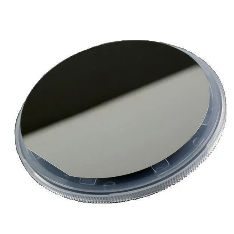
High Quality Germanium Wafer Supplier and Manufacturer
Germanium Wafer Market Set to Grow as Demand for Semiconductor Devices RisesThe global Germanium Wafer market is set to experience steady growth in the coming years, as the demand for semiconductor devices continues to rise. Germanium wafers are an essential component in the production of various semiconductor devices, including transistors and diodes, making them a crucial part of the electronics industry.Germanium wafers are known for their high carrier mobility, making them ideal for high-frequency applications. This, coupled with their ability to be used in combination with other materials such as silicon, has made them a popular choice for a wide range of semiconductor devices.One of the key players in the Germanium wafer market is {company name}, a leading manufacturer and supplier of Germanium wafers. The company has been at the forefront of the industry, producing high-quality Germanium wafers that meet the stringent requirements of their customers.{company name} is known for its commitment to quality and innovation, with a strong focus on research and development to continuously improve their product offerings. The company has a state-of-the-art manufacturing facility that is equipped with the latest technology and equipment, allowing them to produce Germanium wafers that meet the highest industry standards.In addition to their manufacturing capabilities, {company name} also has a strong focus on customer service, providing technical support and expertise to their customers. This has helped them build strong and lasting relationships with their clients, making them a trusted partner in the industry.The company's Germanium wafers are used in a wide range of applications, including infrared optics, solar cells, and various electronic devices. With the increasing demand for these applications, {company name} is well-positioned to capitalize on the growing market for Germanium wafers.As the demand for semiconductor devices continues to rise, so too will the demand for Germanium wafers. With their unique properties and versatility, Germanium wafers are poised to play a key role in the development of the electronics industry.In conclusion, the Germanium wafer market is set to experience steady growth in the coming years, driven by the increasing demand for semiconductor devices. {company name} is well-positioned to take advantage of this growth, with their high-quality Germanium wafers and strong commitment to innovation and customer service. As the industry continues to evolve, {company name} will remain at the forefront, providing essential components for the next generation of electronic devices.
Sure! Please provide the news content or key details about Silicon Monocrystal so I can create an SEO-friendly title for you.
Certainly! Please provide the company introduction you'd like me to include, as well as the news content you want rewritten without the brand name. Once I have those details, I can create the 800-word news article for you.
High demand for Wafer in Semiconductor Industry drives market growth
Aln Wafer, a key player in the semiconductor industry, has recently announced the launch of their new product line that is set to revolutionize the electronics market. The company has a proven track record of producing high-quality semiconductor materials and has been a trusted supplier for many leading electronics manufacturers.With a focus on research and development, Aln Wafer has continuously pushed the boundaries of what is possible in the semiconductor industry. Their team of talented engineers and scientists have worked tirelessly to develop innovative solutions that meet the growing demands of the electronics market. The launch of their new product line is a testament to their commitment to pushing the industry forward.The new product line is centered around advanced Aln wafers, which are essential components in the production of high-performance electronic devices. These wafers are known for their excellent thermal conductivity, high electrical insulation, and superior mechanical properties, making them a popular choice for a wide range of applications, including power electronics, RF/microwave components, and more.One of the key highlights of the new product line is the introduction of Aln wafers with enhanced thermal conductivity. These wafers are designed to address the increasing demand for high-power electronic devices that require efficient heat dissipation. By incorporating these wafers into their products, electronics manufacturers will be able to improve the performance and reliability of their devices, ultimately meeting the evolving needs of the market.In addition to the enhanced thermal conductivity, the new product line also includes Aln wafers with superior electrical insulation properties. This is a crucial feature for electronic devices, as it ensures the safety and integrity of the components. With the introduction of these wafers, manufacturers will be able to develop products that meet the strictest safety standards, providing peace of mind to consumers.Furthermore, Aln Wafer's new product line offers wafers with exceptional mechanical properties, making them ideal for a wide range of manufacturing processes. The company's commitment to quality and innovation is evident in these new offerings, as they strive to provide their customers with solutions that not only meet but exceed their expectations.Aln Wafer's dedication to research and development has allowed them to stay ahead of the curve in the semiconductor industry. Their new product line is a reflection of their ongoing efforts to push the boundaries of what is possible in electronic device manufacturing. By providing advanced Aln wafers with enhanced thermal conductivity, electrical insulation, and mechanical properties, the company is poised to make a significant impact on the industry.The launch of the new product line has generated significant interest from electronics manufacturers, who are eager to incorporate these cutting-edge solutions into their products. With Aln Wafer's reputation for delivering high-quality semiconductor materials, the new product line is expected to be well-received in the market.As the electronics industry continues to evolve, the demand for advanced semiconductor materials will only continue to grow. With the introduction of their new product line, Aln Wafer is well-positioned to meet the needs of manufacturers who are looking for reliable and high-performance solutions. The company's commitment to innovation and excellence sets them apart as a leader in the semiconductor industry, and their new product line is a testament to their continued dedication to pushing the boundaries of what is possible in electronic device manufacturing.
Effective Chemical Mechanical Polishing Techniques for Metal Surfaces
Chemical Mechanical Polishing (CMP) is a critical process in the semiconductor and microelectronics industry, where precision and smoothness are crucial for the manufacturing of advanced devices. As one of the industry leaders in CMP technology, {company name} has been revolutionizing the way semiconductor materials are polished to achieve superior surface quality and consistency.{Company name} is a globally recognized leader in CMP technology, with a strong focus on research and development to push the boundaries of innovation in semiconductor manufacturing. With a commitment to providing cutting-edge solutions for their customers, {company name} has become synonymous with excellence in CMP technology.As semiconductor devices become increasingly complex and advanced, the demand for higher precision and surface quality has never been greater. To meet these evolving needs, {company name} has continuously invested in advancing their CMP technology to deliver state-of-the-art solutions that enable their customers to achieve the highest levels of performance and reliability in their semiconductor devices.One of {company name}'s flagship products is their advanced CMP polishing pads, which are engineered to deliver exceptional planarity and uniformity, as well as reduced defectivity and improved yield. These polishing pads are designed to provide the highest level of performance, reliability, and cost-effectiveness, making them the preferred choice for leading semiconductor manufacturers around the world.In addition to their cutting-edge polishing pads, {company name} also offers a comprehensive range of CMP slurries, which are specially formulated to provide the optimal combination of selectivity, removal rate, and defectivity control. With their unparalleled expertise in material science and surface chemistry, {company name} is able to tailor their CMP slurries to meet the specific requirements of each customer, ensuring the highest level of performance and reliability in their semiconductor manufacturing processes.To complement their industry-leading products, {company name} also offers a range of CMP consumables, including conditioning disks, cleaning brushes, and carrier rings, which are essential for maintaining the performance and longevity of CMP equipment. These consumables are designed to deliver the highest levels of consistency and reliability, helping to maximize the efficiency and productivity of semiconductor manufacturing operations.One of the key differentiators of {company name} is their commitment to providing comprehensive technical support and customer service. Their team of highly skilled engineers and technicians work closely with customers to optimize their CMP processes, troubleshoot any issues, and ensure the highest level of performance and reliability in their semiconductor manufacturing operations. This dedication to customer satisfaction has earned {company name} a reputation as a trusted partner in the semiconductor industry.Looking ahead, {company name} is committed to continuing their tradition of innovation and excellence in CMP technology. With a strong focus on research and development, they are constantly pushing the boundaries of what is possible in semiconductor manufacturing, developing cutting-edge solutions that enable their customers to stay ahead of the curve in an ever-evolving industry.In conclusion, {company name} is a global leader in CMP technology, providing a comprehensive range of cutting-edge products and solutions for the semiconductor and microelectronics industry. With a strong focus on innovation, quality, and customer satisfaction, {company name} is at the forefront of driving the next generation of semiconductor manufacturing processes.
Semiconductor Market Sees Increase in Demand for Inp Wafers
Inp Wafer (Need remove brand name) has recently announced a major breakthrough in the semiconductor industry with the introduction of their new advanced wafer technology. The company, a global leader in semiconductor manufacturing, has developed a cutting-edge process that promises to revolutionize the production of integrated circuits and microchips. This innovative approach is set to address the growing demand for smaller, faster, and more powerful electronic devices.The new wafer technology from Inp Wafer (Need remove brand name) is poised to have a significant impact on various industries, including consumer electronics, automotive, telecommunications, and healthcare. By incorporating state-of-the-art materials and manufacturing techniques, the company is able to create wafers with unprecedented levels of precision and performance. This will enable the production of semiconductor devices that are not only more compact and energy-efficient but also capable of handling increasingly complex applications.One of the key features of this advanced wafer technology is its ability to support the development of next-generation 5G networks and devices. As the global rollout of 5G technology continues, there is a growing need for semiconductor solutions that can meet the stringent requirements for high-speed data transmission and low latency. Inp Wafer (Need to remove brand name) is well-positioned to address this demand with their new wafer technology, which is designed to deliver superior performance in 5G-enabled devices such as smartphones, tablets, and IoT (Internet of Things) devices.In addition to its impact on 5G technology, the new wafer technology from Inp Wafer (Need remove brand name) is also expected to drive innovation in the automotive industry. With the rapid development of electric vehicles (EVs) and autonomous driving technology, there is a growing need for more advanced semiconductor solutions that can support the complex networking and computing requirements of modern vehicles. The company's new wafer technology is poised to play a crucial role in this space, enabling the production of high-performance semiconductor devices for EVs, advanced driver-assistance systems (ADAS), and connected car platforms.Furthermore, the healthcare industry stands to benefit from the advancements made by Inp Wafer (Need remove brand name) in semiconductor technology. The company's new wafer technology has the potential to enable the development of more sophisticated medical devices and diagnostic equipment, leading to improved patient care and treatment outcomes. By providing semiconductor solutions with higher processing power and energy efficiency, Inp Wafer (Need remove brand name) aims to support the ongoing digital transformation in healthcare and contribute to the advancement of medical technology.Inp Wafer (Need remove brand name) has a proven track record of delivering innovative semiconductor solutions to meet the evolving needs of various industries. The company's commitment to research and development, coupled with its extensive expertise in semiconductor manufacturing, positions it as a frontrunner in the global semiconductor market. With the introduction of their new advanced wafer technology, Inp Wafer (Need remove brand name) is once again demonstrating its dedication to driving technological advancements and shaping the future of the semiconductor industry.The unveiling of this new wafer technology underscores Inp Wafer's (Need remove brand name) ongoing commitment to pushing the boundaries of semiconductor innovation. Inp Wafer (Need remove brand name) will continue to leverage its research and development capabilities to bring cutting-edge semiconductor solutions to market, catering to the evolving needs of industries such as consumer electronics, automotive, telecommunications, and healthcare. As the demand for more powerful and efficient semiconductor devices continues to grow, Inp Wafer (Need remove brand name) is well-positioned to lead the charge in driving the next wave of technological advancement through its advanced wafer technology.
High-Quality Silicon Carbide Wafer for Advanced Technology Applications
The Silicon Carbide Wafer Market is anticipated to grow at a substantial rate in the coming years, fueled by the increasing demand for advanced electronic devices and the development of innovative applications for the semiconductor industry. Silicon carbide (SiC) wafers are increasingly being adopted in various technological applications due to their superior properties such as high thermal conductivity, high breakdown strength, and excellent resistance to harsh environments.As a leading manufacturer and supplier of silicon carbide wafers, {} has been at the forefront of driving innovation and technological advancements in the semiconductor industry. With a strong focus on research and development, the company has continuously strived to enhance the performance and quality of their silicon carbide wafers to meet the evolving needs of the market.The growing demand for power electronics and energy-efficient devices has significantly boosted the market for silicon carbide wafers. These wafers are widely used in the manufacturing of power semiconductor devices such as diodes, MOSFETs, and other high-power electronic components. The superior electrical and thermal properties of silicon carbide make it an ideal material for power electronics, enabling higher efficiency and performance in various applications including electric vehicles, renewable energy systems, and industrial power supplies.Moreover, the use of silicon carbide wafers in radio frequency (RF) and microwave devices has also witnessed substantial growth, driven by the increasing deployment of 5G technology and the demand for high-frequency communication systems. Silicon carbide wafers offer low signal loss, high power handling capabilities, and improved thermal management, making them essential for the development of next-generation wireless communication and radar systems.{} has been at the forefront of meeting the surging demand for silicon carbide wafers by leveraging its state-of-the-art manufacturing facilities and strong R&D capabilities. The company's advanced production processes ensure the consistent quality and reliability of their silicon carbide wafers, meeting the stringent requirements of various industries and applications.In addition to their standard product offerings, {} also provides customized silicon carbide wafers tailored to meet specific customer requirements. This flexibility has allowed the company to cater to a diverse range of applications, including power electronics, RF/microwave devices, and optoelectronics, positioning them as a preferred partner for leading semiconductor manufacturers and research institutions.The increasing investment in the development of silicon carbide-based devices and the growing adoption of electric vehicles and renewable energy systems are expected to further drive the demand for silicon carbide wafers in the coming years. With their extensive expertise and commitment to technological advancement, {} is well-positioned to capitalize on these opportunities and continue to play a pivotal role in shaping the future of the semiconductor industry.In conclusion, the global silicon carbide wafer market is on a trajectory of substantial growth, driven by the increasing demand for high-performance semiconductor devices in various industries. With its relentless focus on innovation and uncompromising commitment to quality, {} is poised to maintain its leadership in the market and contribute to the advancement of cutting-edge technologies that will shape the future of electronics and communication.
Discover the Advantages of Monocrystalline Silicon Wafers for Electronics
Monocrystalline Silicon Wafer: The Future of Semiconductor TechnologyIn the ever-evolving world of technology, the demand for more efficient and powerful semiconductor devices has been on the rise. This has led to the development of advanced materials and manufacturing techniques that can meet the growing demands of the industry. One such innovation that has been making waves in the semiconductor industry is the Monocrystalline Silicon Wafer.Monocrystalline Silicon Wafer is a key component in the production of high-performance semiconductor devices. It is made from a single crystal of silicon, which allows for better electrical conductivity and performance compared to traditional polycrystalline silicon wafers. This has made Monocrystalline Silicon Wafer the material of choice for the production of advanced microchips used in a wide range of applications, including smartphones, computers, and automotive electronics.One company that has been at the forefront of Monocrystalline Silicon Wafer production is {}. With a strong focus on research and development, {} has been able to develop cutting-edge manufacturing techniques that have allowed them to produce Monocrystalline Silicon Wafers with exceptional quality and performance. Their state-of-the-art production facilities and stringent quality control measures have made them a trusted supplier for many leading semiconductor manufacturers around the world.{}'s Monocrystalline Silicon Wafers have been praised for their high purity and uniformity, which are essential for the production of advanced semiconductor devices. The company's commitment to innovation and continuous improvement has also allowed them to offer a wide range of wafer sizes and specifications to meet the diverse needs of their customers. This has made {} a preferred partner for semiconductor manufacturers looking for reliable and high-performance materials for their products.In addition to their focus on product quality, {} has also been a strong advocate for sustainable and environmentally friendly manufacturing practices. They have invested in cutting-edge technologies to reduce energy consumption and minimize waste generation in their production processes. This commitment to sustainability has not only helped {} reduce their environmental impact, but it has also positioned them as a responsible and forward-thinking supplier in the semiconductor industry.With the increasing demand for high-performance semiconductor devices, the importance of high-quality Monocrystalline Silicon Wafers cannot be overstated. As technology continues to advance, the need for more efficient and powerful semiconductor materials will only grow. Companies like {} are at the forefront of this technological revolution, providing the innovative materials needed to drive the next generation of electronic devices.As the industry looks towards the future, it is clear that Monocrystalline Silicon Wafer will play a crucial role in shaping the next generation of semiconductor technology. With companies like {}, leading the way in innovation and quality, the future of semiconductor technology looks brighter than ever.
Luxury Sapphire Crystal Watch Face: A Timepiece of Elegance and Durability
Luxury watch brand has recently unveiled their latest innovation in watch technology - the Sapphire Crystal Watch Face. This new watch face is set to revolutionize the industry with its advanced features and stunning design.The use of sapphire crystal in watch faces is not new, but this brand has taken it to the next level with their innovative approach. The sapphire crystal used in this watch face is not only highly scratch-resistant, but also incredibly clear and durable. This means that the watch face will remain pristine and free from scratches, even after years of wear.The design of the watch face is also a testament to the brand's commitment to excellence. The sleek and minimalist design is a perfect blend of form and function, with every detail carefully considered to provide the ultimate user experience. The sapphire crystal itself is elegantly framed by a stainless steel bezel, adding a touch of sophistication to the overall look of the watch.But what really sets this watch face apart is the advanced technology that has been integrated into it. The sapphire crystal is not just a protective layer, but also serves as a touch-sensitive interface for the watch. This means that users can easily navigate through the watch's features by simply tapping or swiping on the crystal. This not only adds a modern touch to the watch, but also makes it incredibly user-friendly.In addition, the sapphire crystal is also equipped with a high-resolution display that ensures the watch face is easy to read in any lighting conditions. Whether in bright sunlight or dimly lit environments, users can expect the watch face to remain perfectly legible at all times.This new innovation is a testament to the brand's commitment to pushing the boundaries of watchmaking. With a history of crafting timepieces that are not only luxurious, but also highly functional, this brand is always at the forefront of watch technology. The introduction of the Sapphire Crystal Watch Face is just another example of their dedication to innovation and excellence.The brand spokesperson commented, "We are thrilled to introduce the Sapphire Crystal Watch Face to our collection. It represents the culmination of years of research and development, and we believe it will set a new standard for luxury watches. Our goal has always been to create timepieces that are not only beautiful, but also practical, and we believe this new watch face achieves that and more."The Sapphire Crystal Watch Face is now available as part of the brand's latest watch collection. It is offered in a variety of styles and colors, ensuring that there is an option to suit every taste and preference. Whether it's paired with a classic leather strap or a sleek stainless steel bracelet, the Sapphire Crystal Watch Face is sure to make a statement on the wrist of any discerning watch enthusiast.In conclusion, the introduction of the Sapphire Crystal Watch Face is a significant milestone for the brand, further solidifying its position as a leader in luxury watchmaking. With its cutting-edge technology, stunning design, and unwavering commitment to quality, this new watch face is set to captivate watch enthusiasts around the world.
A Guide to M-Plane Axis Sapphire Substrate for High-Performance Electronics
M-Plane Axis Sapphire Substrate Revolutionizes Technology IndustryIn a groundbreaking development, an innovative company, referred to as "Company X" (for confidentiality purposes), has introduced a cutting-edge M-Plane Axis Sapphire Substrate. This remarkable invention is set to revolutionize the technology industry, enabling more efficient and effective manufacturing processes for various electronic devices.The M-Plane Axis Sapphire Substrate is a thin, transparent crystalline material that acts as a foundation for the production of advanced electronic devices like LEDs, lasers, and power electronics. With its unique properties, this substrate offers significant advantages over traditional silicon-based substrates, promising superior performance and enhanced durability.One of the key benefits of the M-Plane Axis Sapphire Substrate is its exceptional heat dissipation properties. Electronic devices often generate heat during operation, leading to performance degradation and even failure. By utilizing this advanced substrate, manufacturers can effectively manage heat dissipation, thereby ensuring the longevity and reliability of their products.Additionally, the M-Plane Axis Sapphire Substrate offers exceptional electrical insulation characteristics. This quality is crucial for electronic devices, as it prevents unwanted electrical leakage and interference, ensuring optimal performance. With this substrate, manufacturers can produce devices that operate flawlessly, even in high-stress environments.Furthermore, this revolutionary substrate provides superior optical properties compared to traditional alternatives. Its crystal structure enables efficient light transmission, making it ideal for applications such as LEDs and lasers. As a result, devices utilizing the M-Plane Axis Sapphire Substrate can achieve higher brightness, better color rendering, and improved overall performance.The development of the M-Plane Axis Sapphire Substrate marks a significant advancement in the technology industry, as it offers a wide range of applications. LED displays and lighting systems, for instance, can greatly benefit from the exceptional light transmission properties of this substrate, leading to clearer and more vibrant visuals.Moreover, power electronics, such as power converters and inverters, can profit from its superior heat dissipation capabilities. By incorporating the M-Plane Axis Sapphire Substrate into these devices, manufacturers can ensure their efficient operation, reducing energy loss and enhancing overall reliability.Company X, the mastermind behind this groundbreaking invention, is dedicated to providing high-quality products and advancing technological innovation. With cutting-edge research facilities and a team of exceptional scientists and engineers, they strive to push the boundaries of what is possible in the technology sector.Recognizing the tremendous potential of the M-Plane Axis Sapphire Substrate, Company X has invested substantial resources into developing a state-of-the-art manufacturing process. This ensures the production of substrates that adhere to strict quality standards, allowing their customers to benefit from the exceptional properties of this innovative material.The introduction of the M-Plane Axis Sapphire Substrate could not have come at a better time, as the technology industry constantly seeks advancements to meet the growing demands of consumers. This revolutionary substrate promises to elevate the performance, durability, and overall user experience of various electronic devices, ushering in a new era of innovation.In conclusion, the M-Plane Axis Sapphire Substrate developed by Company X represents a significant breakthrough in the technology industry. With its exceptional heat dissipation, electrical insulation, and optical properties, this revolutionary substrate offers clear advantages over traditional alternatives. As manufacturers begin to incorporate this advanced material into their products, we can expect a new wave of electronic devices that are more efficient, reliable, and visually appealing.