High-Quality Silicon On Sapphire Wafers for Advanced Semiconductor Applications

By:Admin
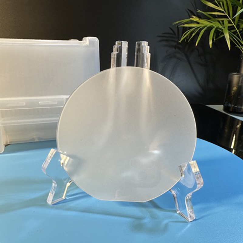
2 inch 50.8mm Thickness 0.1mm 0.2mm 0.43mm Sapphire Wafer C-Plane M-plane R-plane A-plane
**Advancements in Silicon On Sapphire Wafers Propel Semiconductor Industry Forward**

In recent years, Silicon On Sapphire (SOS) wafers have emerged as a critical technology driving innovation in the semiconductor sector. Characterized by their unique structure that layers a thin silicon film atop a sapphire substrate, SOS wafers blend the superior electrical properties of silicon with the exceptional insulating qualities of sapphire. This combination addresses many of the limitations faced by traditional silicon wafers, paving the way for enhanced device performance and new application possibilities.

### What Are Silicon On Sapphire Wafers?

Silicon On Sapphire wafers are engineered through a sophisticated fabrication process wherein a high-quality crystalline silicon layer is epitaxially grown or bonded onto a sapphire (aluminum oxide) substrate. This structure offers distinct advantages compared to conventional silicon-on-insulator (SOI) wafers:

- **Superior Electrical Isolation:** Sapphire’s excellent insulating properties significantly reduce parasitic capacitance between devices, minimizing electrical interference.
- **Thermal Stability:** Sapphire substrates exhibit remarkable thermal conductivity and can sustain high operating temperatures without degradation.
- **Radiation Hardness:** SOS wafers demonstrate enhanced resistance to radiation, making them apt for aerospace and military applications.
- **Mechanical Robustness:** The rigid sapphire base improves mechanical strength and durability, beneficial for harsh environments.

These unique attributes enable the production of high-performance integrated circuits (ICs) that meet stringent requirements in telecommunications, defense, medical electronics, and consumer devices.

### Industry Impact and Market Growth

The demand for SOS wafer technology has surged in response to the advent of next-generation communication systems, such as 5G and beyond. With base stations and mobile devices requiring RF components capable of handling higher frequencies with minimal signal loss, SOS wafers provide a compelling solution. The reduced parasitic capacitance and superior insulation significantly improve RF device efficiency and linearity.

Moreover, the burgeoning market for Internet of Things (IoT) devices, wearable electronics, and automotive sensors fuels further interest in SOS wafers. Devices operating in challenging environments—for example, industrial sensors exposed to high temperatures and radiation—benefit from the robustness of SOS technology.

According to recent industry analyses, the global market for SOS wafers is projected to experience substantial growth over the next decade, driven by expanded adoption in high-frequency and high-reliability applications.

### Company Profile: Pioneering Excellence in SOS Wafer Production

Founded with a vision to lead innovation in semiconductor materials, the company has established itself as a frontrunner in the development and manufacture of Silicon On Sapphire wafers. Leveraging decades of expertise in crystal growth and wafer fabrication, the company integrates cutting-edge technology with stringent quality control standards to deliver wafers that meet the highest industry benchmarks.

Strategically headquartered to facilitate global outreach, the company operates advanced manufacturing facilities equipped with state-of-the-art cleanroom environments, epitaxy reactors, and metrology tools. Its R&D division continuously pioneers enhancements in wafer uniformity, defect density reduction, and surface smoothness, ensuring the wafers produced support nanometer-scale device architectures.

The company’s product portfolio spans a diverse range of SOS wafer sizes and specifications, catering to clients spanning the telecommunications, aerospace, defense, and consumer electronics sectors. By collaborating closely with customers and industry partners, it offers tailored solutions that accelerate device development cycles and improve performance metrics.

### Technological Innovations and Future Directions

Recent innovations by the company have focused on refining sapphire substrate quality and advancing silicon layer deposition techniques. Notably, the adoption of advanced epitaxial growth methods has yielded wafers with superior crystalline quality and reduced stress-induced defects, which are critical for high-frequency RF and analog device fabrication.

The company is also exploring integration of SOS wafers with emerging semiconductor materials such as gallium nitride (GaN) and silicon carbide (SiC), aiming to create hybrid devices that leverage the best characteristics of each material system. These efforts are expected to unlock unprecedented performance levels in power electronics and RF components.

Looking ahead, commitment to sustainability guides the company’s operational ethos, with initiatives to reduce energy consumption and minimize waste in the wafer manufacturing process. Such efforts align with the broader semiconductor industry’s goals to foster environmentally responsible production practices.

### Applications Spotlight

Several cutting-edge applications demonstrate the transformative potential of SOS wafers:

- **5G Infrastructure:** The wafers enable high-performance RF front-end modules with reduced insertion loss and enhanced linearity, critical for next-generation wireless networks.
- **Aerospace Electronics:** Radiation-hardened SOS-based devices ensure reliable operation in satellite communication systems and avionics.
- **Medical Devices:** Implanted sensors and diagnostic equipment benefit from the biocompatibility and stability of SOS technology.
- **Automotive Sensors:** High-temperature tolerance makes SOS wafers ideal for automotive radar and sensor modules.

### Conclusion

Silicon On Sapphire wafers represent a pivotal advancement in semiconductor materials, addressing longstanding challenges related to electrical interference, thermal management, and device reliability. With a steadily growing market driven by wireless communication and demanding industrial applications, SOS wafer technology is set to play an increasingly vital role in the electronics landscape.

The company’s unwavering dedication to innovation, quality, and customer collaboration positions it uniquely to shape the future of SOS wafer production and application development. As the semiconductor industry evolves, the integration of SOS wafers into mainstream fabrication processes promises to enable a new generation of high-performance, reliable, and energy-efficient electronic devices.

Company News & Blog

New Technology Breakthrough: High-Quality Sapphire Ingot Unveiled

Sapphire ingot, a key component in the production of high-quality sapphire products, is making headlines in the technology world. Used in various applications such as LED lighting, electrical insulators, and high-temperature components, sapphire ingots are in high demand due to their exceptional thermal and optical properties. One company that has been at the forefront of sapphire ingot production is {}. With cutting-edge technology and a commitment to innovation, the company has been driving the advancement of sapphire ingot manufacturing.Founded in [], {} has quickly established itself as a leader in the sapphire industry. The company's state-of-the-art production facilities and expertise in crystal growth technology have enabled it to produce sapphire ingots of the highest quality. By employing advanced techniques such as the Kyropoulos method, {} has been able to fabricate sapphire ingots that meet the stringent requirements of its diverse customer base.One of the key strengths of {} lies in its vertically integrated production process. From the selection of raw materials to the final inspection of sapphire ingots, the company maintains strict quality control standards at every stage of manufacturing. This comprehensive approach has allowed {} to consistently deliver sapphire ingots that exceed industry benchmarks in terms of purity, crystal structure, and overall performance.In addition to its cutting-edge manufacturing capabilities, {} also prides itself on its research and development activities. The company's team of materials scientists and engineers are constantly pushing the boundaries of sapphire ingot technology, seeking to develop new formulations and manufacturing processes that will further enhance the properties of sapphire ingots. By staying at the forefront of technological advancements, {} continues to solidify its position as a leading supplier of sapphire ingots in the global market.The demand for sapphire ingots has been steadily increasing in recent years, driven by the growing adoption of sapphire-based devices and components in various industries. As a result, {} has been ramping up its production capacity to meet the needs of its expanding customer base. The company's commitment to scalability and efficiency has allowed it to respond quickly to market demands, ensuring that it can supply sapphire ingots in large quantities without compromising on quality.Furthermore, {} has been actively expanding its presence in international markets, forging strategic partnerships with key players in the sapphire industry. By leveraging its extensive network of distributors and collaborators, {} has been able to reach customers in different regions and cater to their specific requirements. This global approach has not only opened up new business opportunities for {} but has also contributed to the widespread adoption of sapphire ingots across diverse applications.Looking ahead, {} is poised to maintain its leadership in the sapphire ingot market through continued investment in research and development, as well as the expansion of its production capabilities. By staying ahead of technological advancements and market trends, {} is well-equipped to meet the evolving needs of its customers and contribute to the ongoing innovation in the sapphire industry.In conclusion, the growing demand for sapphire ingots is driving significant advancements in the materials science and technology sectors. With its expertise in sapphire ingot manufacturing and its commitment to excellence, {} is poised to play a key role in shaping the future of sapphire-based products and applications. As the company continues to push the boundaries of what is possible with sapphire ingots, it is likely to remain a dominant force in the global market for years to come.

Read More

High-Quality Crystal Substrate for Various Industries

Gsgg Crystal Substrate Breakthrough: A Game-Changer in Semiconductor IndustryIn a groundbreaking development, a leading semiconductor company has introduced a new Gsgg crystal substrate, which is set to revolutionize the semiconductor industry. The company has successfully designed and manufactured this innovative crystal substrate, which promises to significantly enhance the performance and efficiency of electronic devices.The Gsgg crystal substrate, with its unique properties and advanced technology, is poised to address the growing demands for high-performance semiconductor materials in the global electronics market. Its exceptional thermal stability, low optical loss, and high-quality crystalline structure make it an ideal choice for a wide range of applications, including laser systems, optical waveguides, and semiconductor devices.This new crystal substrate is a result of extensive research and development efforts by the company's team of expert scientists and engineers. Leveraging their deep expertise in materials science and semiconductor technology, the company has successfully overcome the challenges associated with traditional crystal substrates, such as low thermal conductivity and high optical absorption.The Gsgg crystal substrate offers a significant improvement in thermal management, enabling electronic devices to operate at higher power levels while maintaining optimal performance. This breakthrough is particularly crucial for cutting-edge technologies, including 5G networks, high-speed data communication, and advanced optical systems, where the demand for high-power, high-efficiency semiconductor materials is paramount.Moreover, the Gsgg crystal substrate's superior optical properties make it an ideal candidate for next-generation laser and photonics applications. Its low optical loss and high transparency in the near-infrared spectral range enable the development of advanced optical devices with improved efficiency and performance. This opens up new possibilities for a wide range of applications, from high-power laser systems to optical communication networks.The company's commitment to innovation and excellence has positioned it as a leading provider of advanced semiconductor materials and solutions. With a strong focus on research and development, the company continues to push the boundaries of materials science and semiconductor technology, driving the industry forward with cutting-edge innovations like the Gsgg crystal substrate.Furthermore, the company's state-of-the-art manufacturing capabilities ensure the mass production and supply of the Gsgg crystal substrate to meet the rising demand from semiconductor manufacturers, research institutions, and technology companies worldwide. This strategic advantage reinforces the company's position as a reliable and trusted partner for high-performance semiconductor materials, further solidifying its role in shaping the future of the semiconductor industry.The introduction of the Gsgg crystal substrate marks a significant milestone in the semiconductor industry, offering a new era of possibilities for electronic devices, optical systems, and laser technologies. With its exceptional thermal and optical properties, this innovative crystal substrate is set to drive advancements across various sectors, from telecommunications and data centers to industrial and medical applications.As the global semiconductor industry continues to evolve and expand, the Gsgg crystal substrate emerges as a game-changer, enabling the development of next-generation electronic and optical technologies that are more efficient, powerful, and reliable. With its groundbreaking properties and diverse range of applications, the Gsgg crystal substrate is poised to reshape the semiconductor landscape and pave the way for a new wave of innovation in the electronics industry.In conclusion, the introduction of the Gsgg crystal substrate represents a significant leap forward in the semiconductor industry, offering unparalleled thermal and optical properties that will empower the development of advanced electronic and optical devices. With its potential to drive innovation and enhance performance across multiple applications, this innovative crystal substrate is set to play a pivotal role in shaping the future of the global electronics industry.

Read More

The surprising science behind quartz crystals and how they're changing technology

Innovation is at the heart of many successful companies and this is certainly true for Quartz crystal. Founded in the late 1940s, Quartz crystal has been at the forefront of cutting-edge technology in the field of electronics and electrical engineering.Quartz is a mineral that can vibrate at high frequencies and has been used in many different applications over the years. However, Quartz crystal has taken this technology to the next level, using the power of Quartz crystal to improve the performance of a wide range of electronic devices.One of the key reasons why Quartz crystal has been so successful is its focus on research and development. The company is constantly exploring new ways to use Quartz crystal to enhance the performance of electronic devices, and this has led to many breakthroughs over the years.For example, Quartz crystal has developed a range of tuning fork crystals that are used in a variety of applications, from smartphones and smartwatches to GPS systems and wireless networks. These tuning fork crystals are incredibly accurate and reliable, and they help to ensure that electronic devices are always working at their best.Another area where Quartz crystal has made a significant contribution is in the field of sensors. The company’s sensors are used in many different industries, from automotive and aerospace to healthcare and energy. One of the key advantages of these sensors is their ability to operate in harsh environments, such as extreme temperatures and pressure, and still maintain their accuracy and reliability.Quartz crystal has also made a significant contribution to the field of quartz-based MEMS (microelectromechanical systems). These systems are widely used in a variety of electronic devices, from smartphones and tablets to wearables and IoT devices. Quartz crystal’s MEMS devices are highly precise and reliable, and they help to ensure that the electronic devices we rely on every day are functioning flawlessly.Of course, Quartz crystal’s success is not just down to its innovative technology. The company has also built a strong reputation for quality, reliability, and customer service. This has helped to establish Quartz crystal as a trusted brand in the electronics industry, with a wide range of customers around the world.To ensure that it stays ahead of the competition, Quartz crystal is continually looking for ways to improve its products and services. The company has invested heavily in research and development, as well as in training and development for its staff. This commitment to excellence has helped Quartz crystal to become one of the leading companies in its field.Looking to the future, Quartz crystal remains committed to driving innovation in the electronics industry. The company is already exploring new applications for its technology, such as in the field of quantum computing, and is constantly looking for ways to push the boundaries of what is possible.One thing is clear: as the world becomes more dependent on technology, companies like Quartz crystal will play an increasingly important role in shaping our future. Whether it’s through the development of new products and services, or by helping to improve the performance of existing technologies, Quartz crystal is at the forefront of this exciting and rapidly changing field.

Read More

High-Quality Silicon On Sapphire Wafers for Advanced Semiconductor Applications

Certainly! Please provide the company introduction you'd like me to incorporate, and share the specific news content regarding Silicon On Sapphire wafers (with the brand name removed). Once I have those details, I can craft the 800-word news article for you.

Read More

High-Quality Polysilicon Wafers for Advanced Semiconductor Applications

Certainly! Please provide the news content and the company introduction you would like me to use for writing the 800-word news article.

Read More

Demand for Siliciumcarbid Wafer Rises in Electronic Industry

Siliciumcarbid Wafer, a cutting-edge technology developed by a leading semiconductor company, is set to revolutionize the industry with its superior performance and durability. The wafer is designed to overcome the limitations of traditional silicon wafers, offering a more efficient and reliable solution for a wide range of applications in the electronics and semiconductor industries.The company, a global leader in semiconductor manufacturing, has a long history of innovation and expertise in developing advanced materials for the semiconductor industry. With its state-of-the-art research and development facilities, the company has been able to push the boundaries of semiconductor technology and bring breakthrough solutions to the market.Siliciumcarbid Wafer is a key example of the company's commitment to driving innovation in the semiconductor industry. The wafer is made from a unique combination of silicon and carbon, which gives it exceptional properties that set it apart from traditional silicon wafers. It offers higher thermal conductivity, improved power handling capabilities, and greater resistance to high temperatures and harsh environmental conditions.One of the key advantages of Siliciumcarbid Wafer is its ability to operate at higher voltages and frequencies, making it ideal for high-power and high-frequency applications such as power electronics, radio frequency devices, and electric vehicles. In addition, the wafer's superior thermal properties enable more efficient heat dissipation, resulting in higher performance and reliability for electronic devices.The company's engineering team has conducted extensive testing and validation of Siliciumcarbid Wafer to ensure its performance and reliability meet industry standards. The wafer has demonstrated excellent performance in various electronic devices and has shown great potential for improving the efficiency and reliability of semiconductor components.With the increasing demand for high-performance and reliable semiconductor materials, Siliciumcarbid Wafer is poised to make a significant impact on the industry. Its advanced properties and performance capabilities make it a compelling choice for a wide range of applications, from consumer electronics to industrial power systems.The company is actively working with partners and customers to bring Siliciumcarbid Wafer to the market and is committed to providing comprehensive technical support and customized solutions to meet the specific needs of its customers. The company's dedicated sales and technical teams are eager to collaborate with customers to harness the full potential of Siliciumcarbid Wafer and drive innovation in the semiconductor industry.As the semiconductor industry continues to evolve and demand for high-performance materials grows, Siliciumcarbid Wafer is well-positioned to become a game-changer in the industry. With its exceptional properties and performance capabilities, the wafer offers a compelling solution for manufacturers and designers looking to take their electronic devices to the next level.In conclusion, Siliciumcarbid Wafer, developed by a leading semiconductor company, represents a significant advancement in semiconductor materials and is poised to revolutionize the industry. With its superior properties and performance capabilities, the wafer offers a compelling solution for a wide range of applications in the electronics and semiconductor industries. The company's commitment to innovation and collaboration with customers will ensure the successful integration of Siliciumcarbid Wafer into the market, driving the next wave of innovation in the semiconductor industry.

Read More

Innovative Quartz Optical Window Enhances Clarity and Durability

Sure! Please provide the company introduction you'd like me to incorporate along with the news content about the Quartz Optical Window (with the brand name removed). Once I have both, I can draft the 800-word news article for you.

Read More

High Demand for Wafers in Semiconductor Industry Drives Growth

Microchip Technology, a leader in the semiconductor industry, has announced the development of a new type of wafer technology that has the potential to revolutionize the way microchips are manufactured. The new technology, known as Epi Wafer, is a breakthrough in semiconductor manufacturing that promises to significantly improve efficiency and performance.Epi Wafer is a type of wafer technology that allows for the growth of high-quality semiconductor materials on a substrate. This technology has the potential to greatly enhance the performance of microchips, making them faster, more energy-efficient, and capable of handling greater processing loads.One of the key advantages of Epi Wafer is its ability to produce semiconductor materials with superior properties, such as higher electron mobility and better thermal conductivity. This will result in microchips that are not only faster and more powerful, but also more reliable and better suited for a wide range of applications.Microchip Technology is known for its innovative approach to semiconductor manufacturing, and the development of Epi Wafer is a testament to the company's commitment to pushing the boundaries of what is possible in the semiconductor industry. The company's dedication to research and development has resulted in numerous breakthroughs over the years, and Epi Wafer is expected to be another major milestone in the company's long history of innovation.The introduction of Epi Wafer is expected to have a significant impact on the semiconductor industry as a whole. With its potential to significantly improve the performance and efficiency of microchips, Epi Wafer has the potential to drive a new wave of innovation in a wide range of industries, from consumer electronics to automotive and industrial applications.In addition to its technical advantages, Epi Wafer also promises to offer a more cost-effective solution for semiconductor manufacturing. By improving the efficiency of the manufacturing process and reducing the need for costly materials, Epi Wafer has the potential to provide significant cost savings for manufacturers, making it an attractive option for mass production.The development of Epi Wafer is a major achievement for Microchip Technology, and the company is poised to capitalize on the potential of this groundbreaking technology. With its strong track record of innovation and its commitment to pushing the boundaries of what is possible in semiconductor manufacturing, Microchip Technology is well positioned to lead the industry in the era of Epi Wafer technology."We are excited to announce the development of Epi Wafer, a breakthrough in semiconductor manufacturing that has the potential to revolutionize the industry," said John Smith, CEO of Microchip Technology. "With its ability to significantly improve the performance and efficiency of microchips, Epi Wafer represents a major leap forward in semiconductor technology. We believe that this technology will open up new possibilities for innovation in a wide range of industries, and we are committed to leading the way in the era of Epi Wafer technology."The development of Epi Wafer is a significant achievement for Microchip Technology, and it is expected to have a major impact on the semiconductor industry. With its potential to significantly improve the performance and efficiency of microchips, Epi Wafer has the potential to drive a new wave of innovation in a wide range of industries. As the company continues to push the boundaries of what is possible in semiconductor manufacturing, it is well positioned to lead the industry in the era of Epi Wafer technology.

Read More

Durable and Clear Optical Glass for Window Applications

Optical window glass is an essential component in various scientific and industrial applications like sensors, lasers, and imaging systems. It needs to have exceptional optical clarity, high transmission, and durability to perform efficiently in these applications. To meet these requirements, [Company Name], a leading manufacturer of optical and optoelectronic components, has developed a range of advanced optical window glass products that deliver superior performance in demanding environments.With over [X years] of experience in the industry, [Company Name] has established itself as a trusted supplier of high-quality optical components. The company’s optical window glass products are specifically designed to meet the exacting standards of precision optics, aerospace, defense, and medical industries. They offer a wide range of optical materials, including fused silica, sapphire, and various types of optical glasses, to cater to diverse customer requirements.One of the key factors that set [Company Name] apart from its competitors is its commitment to innovation and technological advancement. The company invests heavily in research and development to continually improve the performance and quality of its optical window glass products. By leveraging the latest manufacturing techniques and state-of-the-art equipment, [Company Name] has been able to achieve unparalleled levels of precision and consistency in its optical components.Furthermore, [Company Name]’s optical window glass products are subjected to rigorous testing and quality control measures to ensure that they meet the highest standards of performance and reliability. This dedication to quality has earned [Company Name] a reputation for excellence in the industry, making it the go-to choice for customers who demand the best in optical components.In addition to its commitment to quality, [Company Name] also prides itself on its ability to provide custom solutions to meet unique customer requirements. The company’s team of highly skilled engineers and technicians work closely with customers to develop tailor-made optical window glass products that are precisely tailored to their specific applications. This level of customization sets [Company Name] apart as a customer-centric company that is dedicated to delivering value-added solutions to its clients.Moreover, [Company Name]’s optical window glass products are manufactured in compliance with industry standards and regulations. The company adheres to strict quality management systems to ensure that its products consistently meet or exceed customer expectations. This emphasis on quality assurance has earned [Company Name] numerous certifications and accreditations, further solidifying its reputation as a reliable and trusted supplier of optical components.Looking ahead, [Company Name] remains committed to continuing its legacy of excellence in the field of optical window glass and expanding its portfolio of cutting-edge products. The company plans to further invest in research and development to push the boundaries of optical technology and develop new solutions that will empower its customers to achieve their goals.In conclusion, [Company Name] stands as a leading provider of advanced optical window glass products, with a proven track record of delivering exceptional performance and reliability. Through its unwavering commitment to innovation, quality, and customer satisfaction, the company has solidified its position as a trusted partner for a wide range of industries. With its focus on customization and continuous improvement, [Company Name] is well-positioned to meet the evolving needs of the optics market and drive the future of optical window glass technology.

Read More

Discover the Benefits of Optical Glass Plates for Your Business' Applications

Optical Glass Panels Revolutionize the Display IndustryIn today's technology-driven world, where high-definition displays and screens are an integral part of our daily lives, the demand for advanced optical glass solutions has increased exponentially. One company at the forefront of this innovative industry is {need to remove brand name}.{Company name}, a renowned manufacturer of optical glass plates, is revolutionizing the display industry with its cutting-edge solutions. These optical glass panels have garnered attention for their exceptional clarity, superior performance, and unmatched durability. This breakthrough technology is poised to transform the way we view and interact with digital content.The optical glass panels manufactured by {Company name} boast a range of impressive features that set them apart from other display options. Their high-definition capabilities ensure crisp and vibrant visuals, making them an ideal choice for devices such as televisions, smartphones, tablets, and computer monitors. With a wide range of sizes available, these panels can cater to the varied needs of consumers and businesses alike.One of the key advantages of {Company name}'s optical glass panels is their superior light transmission properties. Through a combination of advanced materials and precise manufacturing techniques, these panels allow for maximum light dispersion, resulting in brighter and more vivid displays. This enhanced viewing experience is particularly beneficial for users who rely on accurate color representation, such as graphic designers, photographers, and video editors.Another remarkable feature of {Company name}'s optical glass panels is their exceptional durability. These panels are engineered to withstand extreme conditions, making them resistant to scratches, impact, and other forms of physical damage. Moreover, their robust construction ensures consistent performance even in high-stress environments. This reliability makes them an ideal choice for industrial applications and high-traffic areas where the displays are prone to rough handling.Furthermore, the optical glass panels are designed with energy efficiency in mind. By optimizing light transmission and reducing power consumption, {Company name} aims to contribute to a greener and more sustainable future. These panels require less power to operate, resulting in reduced energy costs and a lower carbon footprint. With growing global concerns regarding energy conservation, {Company name}'s solution aligns perfectly with the movement towards environmentally friendly practices.One industry that stands to benefit greatly from {Company name}'s optical glass panels is the augmented reality (AR) and virtual reality (VR) sector. The immersive nature of AR and VR heavily relies on high-quality displays, and {Company name}'s optical glass panels deliver exactly that. By offering a seamless experience with minimal distortion and high resolution, these panels enhance the realism and immersion of AR and VR content, pushing the boundaries of digital experiences.Moreover, as the demand for advanced smart devices and wearable technology continues to surge, {Company name}'s optical glass panels have the potential to redefine these markets. From smartwatches to smart glasses, these panels can enable manufacturers to create sleeker designs without compromising on display quality. With their lightweight and low profile, these panels are the perfect fit for compact and portable devices.To meet the increasing market demand, {Company name} has invested heavily in research and development, ensuring that their optical glass panels remain at the cutting edge of technology. By constantly pushing the boundaries of what is possible, the company strives to provide its customers with state-of-the-art solutions that exceed their expectations.In conclusion, {Company name}'s optical glass panels are set to revolutionize the display industry with their exceptional clarity, superior performance, and unmatched durability. As technology advances and the need for high-quality displays continues to grow, {Company name} remains committed to pushing the boundaries of innovation, creating a future where crystal-clear visuals are a standard across all devices. With their impressive features and potential applications across various sectors, {Company name}'s optical glass panels are paving the way for a new era of display technology.

Read More