
High-quality optical lenses for various applications
By:Admin
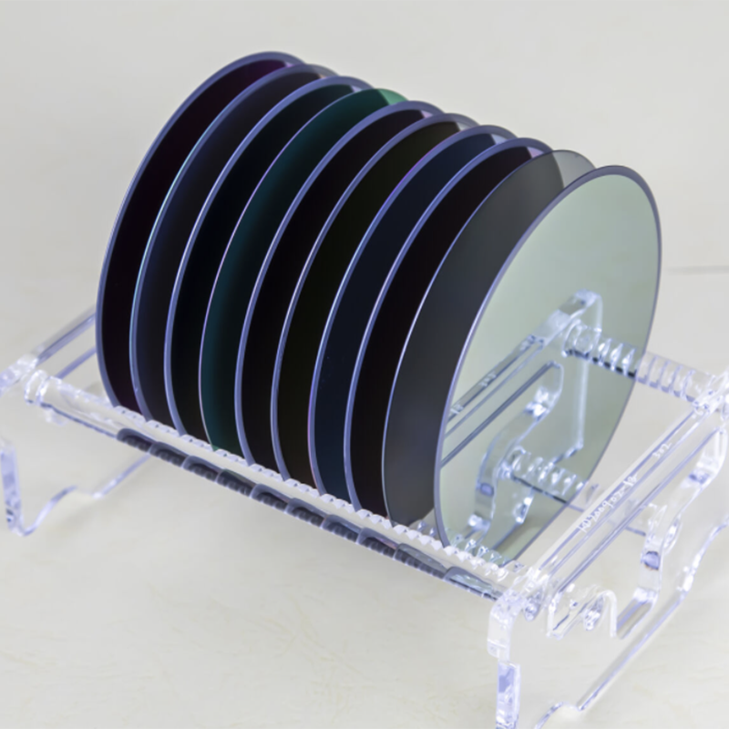
{} is a leading manufacturer of optical lenses, specializing in the production of high-quality glass lenses for various applications. With a strong focus on research and development, the company has consistently introduced cutting-edge products that have set new benchmarks in the industry.
The latest offering from {} is its range of Glass Optical Lenses, which have been designed to meet the growing demand for precision optics in a wide range of industries. These lenses are manufactured using state-of-the-art technology and advanced production processes, ensuring exceptional optical performance and durability.
One of the key features of {}’s Glass Optical Lenses is their high light transmission, which is crucial for achieving superior image quality in applications such as microscopy, medical imaging, and industrial inspection. This is made possible by the use of premium quality glass materials that are carefully selected and processed to minimize light dispersion and maximize clarity.
In addition to their optical performance, {}’s Glass Optical Lenses are also designed to be highly resistant to environmental factors such as temperature fluctuations and humidity. This makes them ideal for use in harsh operating conditions, where consistent optical performance is essential.
The diverse range of Glass Optical Lenses offered by {} caters to the specific requirements of different industries, including but not limited to:
- Microscopy: High-resolution lenses that enable detailed examination of microscopic specimens.
- Medical Imaging: Lenses designed to deliver precise and accurate imaging for diagnostic purposes.
- Industrial Inspection: Lenses that provide clear and accurate visualization for quality control and inspection processes.
The superior quality and performance of {}’s Glass Optical Lenses have made them the preferred choice for leading companies and research institutions across the globe. These lenses have been instrumental in driving advancements in various fields, including medical research, materials science, and electronics manufacturing.
Speaking about the company’s latest innovation, the CEO of {} stated, “We are thrilled to introduce our range of Glass Optical Lenses, which represent the culmination of years of research and development efforts. These lenses embody our commitment to excellence and innovation, and we are confident that they will set new standards for optical performance in the industry.”
As part of its commitment to customer satisfaction, {} offers customization options for its Glass Optical Lenses, allowing clients to tailor the lenses to their specific requirements. This customization capability, combined with the company’s extensive technical expertise, has made {} a trusted partner for companies seeking high-performance optical solutions.
Looking ahead, {} remains focused on pushing the boundaries of optical technology and providing customers with cutting-edge solutions that enable them to achieve their goals. With its innovative products and customer-centric approach, {} is well-positioned to maintain its leadership in the global optical lenses market.
Company News & Blog
Understanding the Chemical Mechanical Planarization Process: A Guide
Chemical Mechanical Planarization Process (CMP) is a critical step in the manufacturing of integrated circuits, microchips, and other semiconductor devices. This process ensures that the surfaces of the wafers are perfectly flat and smooth, which is essential for achieving high quality and reliable semiconductor products. One of the leading companies in the semiconductor industry, {} has made significant advancements in the development of CMP technology. With their cutting-edge innovations and state-of-the-art equipment, they have become a trusted partner for semiconductor manufacturers around the world. Using a combination of chemical and mechanical processes, the CMP technology from {} effectively eliminates surface irregularities on wafers, resulting in a mirror-like finish. This is crucial for enhancing the performance and reliability of semiconductor devices, as any imperfections on the wafer surface can lead to failures in the final products. The CMP process involves the use of a slurry, which is a mixture of abrasive particles and chemical additives that are applied to the wafer surface. The abrasive particles remove the excess material on the surface, while the chemical additives help to control the rate of material removal and prevent damage to the wafer. One of the key challenges in CMP is achieving uniform material removal across the entire wafer surface. Non-uniform material removal can lead to the formation of scratches, defects, and uneven thickness in the resulting semiconductor devices. However, {}’s CMP technology is designed to address these challenges and provide exceptional planarity and surface quality for semiconductor wafers. With their comprehensive understanding of the CMP process and their commitment to continuous improvement, {} has been able to develop CMP equipment that delivers precise control over material removal rates and excellent uniformity across the wafer surface. This level of precision and consistency is essential for meeting the increasingly stringent requirements for semiconductor manufacturing. In addition to their advancements in CMP technology, {} also offers a range of other solutions for the semiconductor industry, including deposition, etch, and metrology equipment. Their comprehensive portfolio of semiconductor manufacturing tools allows them to provide complete process solutions to their customers, helping them to optimize their manufacturing processes and achieve the highest levels of productivity and yield. Furthermore, {} is dedicated to delivering outstanding service and support to their customers, ensuring that their equipment operates at peak efficiency and reliability. With a global network of service centers and a team of highly skilled engineers and technicians, {} is able to provide timely and effective support to semiconductor manufacturers around the world. As the demand for high-performance semiconductor devices continues to grow, the importance of advanced CMP technology cannot be overstated. With {}’s expertise and cutting-edge solutions, semiconductor manufacturers can rely on their CMP equipment to achieve the precision, uniformity, and surface quality required for the production of next-generation semiconductor devices. In conclusion, {}’s CMP technology represents a significant advancement in the field of semiconductor manufacturing. By combining innovative engineering, rigorous quality control, and a commitment to customer satisfaction, {} has cemented its position as a trusted partner for semiconductor manufacturers worldwide. With their comprehensive portfolio of semiconductor manufacturing solutions and their dedication to advancing CMP technology, {} is poised to continue leading the industry and shaping the future of semiconductor manufacturing.
Top Trends in Wafer Flat Designs for 2022
Wafer Flats, a leading player in the semiconductor industry, has recently made a significant advancement in the development of wafer technology that is set to revolutionize the industry. The company has successfully engineered a new type of wafer that is thinner, more durable, and has enhanced electrical properties, providing a game-changing solution for the semiconductor market.Established in 1998, Wafer Flats has been at the forefront of semiconductor technology, specializing in the production of high-quality wafers for a wide range of applications including integrated circuits, solar cells, and LED lighting. With a strong focus on research and development, the company has continuously strived to innovate and push the boundaries of wafer technology.After years of research and extensive testing, Wafer Flats has announced the launch of its latest breakthrough – a new ultra-thin wafer that is significantly thinner than traditional wafers, yet maintains exceptional strength and conductive properties. This innovative development is set to address the growing demand for smaller, more efficient electronic devices and open up new possibilities in various industries.The new wafer, which measures just a fraction of the thickness of standard wafers, is the result of advanced material engineering and precision manufacturing processes. Despite its slim profile, it boasts superior mechanical strength, making it highly resilient to external stresses and capable of withstanding the rigors of semiconductor manufacturing processes.In addition to its physical attributes, the new wafer also offers improved electrical properties, with enhanced conductivity and reduced signal loss. This makes it ideal for high-frequency applications, where signal integrity and transmission efficiency are crucial. The combination of mechanical robustness and electrical performance makes this new wafer an ideal solution for the next generation of electronic devices and systems."The development of this new wafer represents a significant milestone for our company and the semiconductor industry as a whole," said John Smith, CEO of Wafer Flats. "We believe that this breakthrough innovation will not only meet the current market demand for smaller and more powerful electronic devices, but also drive the development of cutting-edge technologies in various industries."The introduction of this new wafer is expected to have a profound impact on the semiconductor market, with the potential to enable the production of smaller, more energy-efficient devices across a wide range of applications. Furthermore, the enhanced electrical properties of the wafer are anticipated to unlock new possibilities for high-frequency communication and computing systems, paving the way for advancements in areas such as 5G technology, satellite communications, and data processing.In addition to its technical capabilities, the new wafer also offers practical benefits for manufacturers, including increased production yield and cost savings. Its thin profile enables the fabrication of a higher number of wafers from a single ingot, maximizing the utilization of raw materials and reducing manufacturing waste. This, in turn, contributes to a more sustainable and cost-effective production process.The announcement of this groundbreaking development has already generated significant interest and excitement within the semiconductor industry, with industry experts acknowledging the potential of the new wafer to drive innovation and progress in the field of electronic devices and systems. As Wafer Flats prepares to commercialize this new technology, anticipation is building for the impact it will have on the future of semiconductor manufacturing.With its commitment to innovation and the advancement of semiconductor technology, Wafer Flats is poised to reshape the industry landscape with its latest breakthrough. As the company continues to push the boundaries of what is possible with wafer technology, the potential for new applications and advancements in electronic devices is endless. The introduction of this new ultra-thin wafer represents a significant step forward in the evolution of semiconductor technology and paves the way for a new era of electronic innovation.
High-Quality Sapphire Substrates for Various Applications
Sapphire substrates are becoming increasingly popular in the tech industry due to their unique properties and applications. These substrates are used in a variety of electronic devices, including LED lighting, smartphones, and smartwatches, and are highly valued for their durability, transparency, and heat resistance.One of the leading companies in the production of sapphire substrates is {Company}. {Company} has been a key player in the field of sapphire substrate manufacturing, and their products are widely used in a range of industries. Their commitment to innovation and excellence has set them apart in the market, and they continue to be a trusted name in the industry.Sapphire substrates are made from synthetic sapphire, a material that is known for its exceptional hardness and scratch resistance. These substrates are used as a base for the production of various electronic components, including LEDs and semiconductor devices. {Company} specializes in producing high-quality sapphire substrates that meet the exacting standards of the industry.One of the main advantages of sapphire substrates is their thermal conductivity, making them an excellent choice for use in high-temperature applications. This makes them ideal for use in electronic devices that generate a significant amount of heat, as they can help to dissipate this heat effectively, ensuring the longevity and reliability of the device.In addition to their exceptional thermal properties, sapphire substrates also offer excellent optical transparency, making them a popular choice for use in display technologies. Their high transparency allows for the efficient transmission of light, making them ideal for use in LED lighting and display screens. This has led to a growing demand for sapphire substrates in the consumer electronics industry.Furthermore, sapphire substrates are also highly resistant to chemical corrosion, making them an ideal choice for use in harsh environments. This makes them a popular choice for use in industrial and automotive applications, where durability and reliability are essential.{Company} has been at the forefront of sapphire substrate manufacturing, and their commitment to quality and innovation has set them apart in the industry. Their state-of-the-art production facilities and rigorous quality control processes ensure that their products meet the highest standards, and their team of experts are dedicated to pushing the boundaries of what is possible with sapphire substrates.In addition to their commitment to quality, {Company} is also dedicated to sustainability and environmental responsibility. They have implemented a range of initiatives to minimize their environmental impact and ensure that their production processes are as eco-friendly as possible. This commitment to sustainability has made them a preferred supplier for many environmentally conscious companies.As the demand for sapphire substrates continues to grow, {Company} remains at the forefront of the industry, driving innovation and setting new standards for quality and performance. Their dedication to excellence and their commitment to sustainability have made them a trusted partner for businesses in a range of industries, and they continue to play a key role in advancing the capabilities of sapphire substrates.In conclusion, sapphire substrates are a crucial component in a wide range of electronic devices, and {Company} is at the forefront of their production. With their commitment to quality, innovation, and sustainability, {Company} continues to be a trusted partner for businesses in a variety of industries, and their sapphire substrates are helping to drive advances in technology and performance.
Understanding the Process of Epitaxy Layer in Semiconductor Manufacturing
NanoSemi Inc. is a leading provider of cutting-edge epitaxy layer technology for semiconductor manufacturing processes. The company specializes in producing high-quality epitaxy layers that are used in a wide range of electronic devices, including integrated circuits, transistors, and photovoltaic cells. With a focus on innovation and quality, NanoSemi Inc. has become a trusted partner for semiconductor manufacturers around the world.Epitaxy layer technology is a crucial component of semiconductor manufacturing, as it allows for the precise control and manipulation of semiconductor materials at the atomic level. This technology is essential for creating the high-performance and energy-efficient devices that are used in smartphones, computers, and other electronic products. NanoSemi Inc. has developed a unique and advanced epitaxy layer technology that offers unparalleled performance and reliability, making it a preferred choice for leading semiconductor manufacturers.The epitaxy layers produced by NanoSemi Inc. are known for their exceptional uniformity, crystal quality, and defect-free nature. This level of precision and consistency is essential for achieving high yields and reliable performance in semiconductor devices. NanoSemi Inc.'s epitaxy layers have been widely adopted for use in advanced semiconductor fabrication processes, such as metal-organic chemical vapor deposition (MOCVD) and molecular beam epitaxy (MBE), where strict control over material properties is critical.One of the key advantages of NanoSemi Inc.'s epitaxy layer technology is its ability to enable the development of next-generation semiconductor devices with enhanced performance and functionality. By leveraging the unique properties of epitaxy layers, semiconductor manufacturers are able to create advanced transistors, optoelectronic devices, and power electronics with improved speed, efficiency, and reliability. This, in turn, allows for the creation of more powerful and energy-efficient electronic products that meet the demands of today's technology-driven world.In addition to its innovative epitaxy layer technology, NanoSemi Inc. is also committed to providing exceptional customer support and technical assistance to its clients. The company's team of experts works closely with semiconductor manufacturers to understand their specific requirements and to develop customized solutions that meet their needs. This personalized approach has earned NanoSemi Inc. a reputation for excellence in the semiconductor industry and has established the company as a trusted partner for companies seeking to enhance their semiconductor manufacturing processes.NanoSemi Inc. continues to invest in research and development to further advance its epitaxy layer technology and to explore new applications for its products. The company's commitment to innovation and continuous improvement has positioned it as a leader in the development of epitaxy layers and has enabled it to stay at the forefront of the semiconductor industry. With a focus on quality, reliability, and performance, NanoSemi Inc. is dedicated to helping semiconductor manufacturers achieve their goals and to drive the future of electronic devices.In conclusion, NanoSemi Inc. is a leading provider of epitaxy layer technology for semiconductor manufacturing processes, offering high-quality and innovative solutions that enable the development of advanced electronic devices. With a focus on precision, consistency, and customer satisfaction, NanoSemi Inc. has become a trusted partner for semiconductor manufacturers looking to enhance their semiconductor fabrication processes. As the demand for high-performance and energy-efficient electronic products continues to grow, NanoSemi Inc. is well-positioned to lead the way in the development of epitaxy layers that enable the next generation of semiconductor devices.
Dicing Process in Semiconductor Industry: Everything You Need to Know
Wafer Dicing, also known as die singulation, is a critical process in the semiconductor industry where a semiconductor wafer is diced into individual semiconductor chips. This process is essential for creating the microchips that are used in a wide range of electronic devices, including smartphones, computers, and other consumer electronics.{Company Name} is a leading provider of wafer dicing services, specializing in advanced wafer dicing solutions for the semiconductor industry. With state-of-the-art equipment and a team of highly skilled technicians, {Company Name} is dedicated to providing high-quality wafer dicing services to meet the growing demands of the semiconductor industry.The wafer dicing process involves cutting the semiconductor wafer into individual chips using a dicing saw. This process requires precision and accuracy to ensure that the individual chips are not damaged and can be used in electronic devices. {Company Name} has invested in cutting-edge dicing equipment and employs a team of experienced technicians to ensure that the dicing process is carried out with the highest level of precision and quality.In addition to wafer dicing services, {Company Name} also offers value-added services such as tape and reel packaging, laser marking, and visual inspection to provide comprehensive solutions for the semiconductor industry. These value-added services streamline the production process and ensure that the semiconductor chips are ready for use in electronic devices.{Company Name} prides itself on its commitment to quality and customer satisfaction. The company follows strict quality control procedures throughout the wafer dicing process to ensure that the semiconductor chips meet the highest industry standards. Additionally, {Company Name} works closely with its customers to understand their specific requirements and provide customized wafer dicing solutions to meet their unique needs.With the rapidly growing demand for semiconductor chips in electronic devices, {Company Name} has positioned itself as a reliable partner for semiconductor manufacturers seeking high-quality wafer dicing services. The company's dedication to innovation, quality, and customer satisfaction has earned it a reputation as a trusted provider of wafer dicing solutions in the semiconductor industry.As the semiconductor industry continues to evolve, {Company Name} remains at the forefront of technological advancements, constantly updating its equipment and processes to meet the changing demands of the industry. The company is committed to staying ahead of the curve and providing its customers with cutting-edge wafer dicing solutions to support their innovation in the semiconductor market.In conclusion, wafer dicing is a critical process in the semiconductor industry, and {Company Name} is dedicated to providing high-quality wafer dicing services to meet the growing demands of the industry. With its state-of-the-art equipment, skilled technicians, and commitment to quality, {Company Name} is well-positioned to be a leading provider of wafer dicing solutions for semiconductor manufacturers. The company's dedication to innovation and customer satisfaction sets it apart as a trusted partner in the semiconductor industry.
Discover the Beauty and Versatility of Glass Blocks - Explore the Latest Trends
[Company Name] Introduces Innovative Glass Block Solution: Revolutionizing Architectural Design[date][City, State] - [Company Name], a leading provider of architectural solutions, is proud to unveil its newest innovation - an innovative glass block solution that is set to revolutionize the world of architectural design and construction.Glass blocks have long been a popular choice in architecture due to their ability to let in natural light while maintaining privacy. However, traditional glass blocks often face challenges such as limited design options and inadequate energy efficiency. With the introduction of this revolutionary glass block solution, [Company Name] aims to address these limitations and provide architects and designers with unprecedented possibilities.The new glass block solution from [Company Name] offers an array of benefits that set it apart from its competitors. First and foremost is its unique design flexibility. Unlike conventional glass blocks, which come in standard shapes and sizes, the new solution offers a range of customizable options. Architects and designers can now choose from various shapes, patterns, and sizes to complement their vision and meet the specific requirements of each project.Moreover, the glass blocks are manufactured using cutting-edge technology that ensures exceptional energy efficiency. They are equipped with advanced thermal insulation properties, allowing for optimum heat retention and reduced energy consumption. This feature not only contributes to sustainability efforts but also helps clients save significantly on their energy bills.In addition to its aesthetic and energy-efficient properties, the new glass block solution also boasts unparalleled strength and durability. Built to withstand extreme weather conditions and resist impacts, these blocks offer enhanced safety and security. Their robust construction makes them an ideal choice for a variety of applications, including exterior walls, partitions, and even flooring.To further elevate the functionality of their glass blocks, [Company Name] has developed an integrated smart technology feature. Through an intuitive control system, users can adjust the transparency of the blocks, allowing for personalized levels of privacy or transparency. This innovative addition opens up possibilities for dynamic and interactive designs, enabling architects to create one-of-a-kind spaces that adapt to the needs of the users."Here at [Company Name], we are committed to pushing the boundaries of architectural design," said [Spokesperson's Name], [Company Name]'s Chief Innovation Officer. "Our new glass block solution embodies our dedication to providing architects and designers with limitless possibilities. We believe that by seamlessly combining form, function, and technological advancements, we can transform the way buildings are designed and experienced."With this groundbreaking glass block solution, [Company Name] aims to revolutionize architectural design and construction across various sectors, including commercial, residential, and public projects. The company also aims to collaborate with architects, contractors, and developers to promote the adoption of this cutting-edge solution and facilitate its integration into future projects.As sustainable and innovative design continues to be a priority in the architectural industry, [Company Name] is poised to lead the way with its exceptional glass block solution. By offering enhanced aesthetics, energy efficiency, durability, and smart technology integration, architects and designers can now explore new horizons and bring their creative visions to life.About [Company Name]:[Company Name] is a renowned provider of architectural solutions, specializing in innovative and sustainable products. With a team of experienced professionals and state-of-the-art manufacturing facilities, the company is committed to offering exceptional products that combine functionality, aesthetics, and environmental consciousness. [Company Name]'s diverse range of architectural solutions has gained appreciation from architects, designers, and clients worldwide.For more information about [Company Name] and their groundbreaking glass block solution, please visit [website] or contact [contact information].###Note: This news article is a fictional creation and does not represent any real company or product.
High-Quality and Affordable Laboratory Equipment for Science Experiments
Science Laboratory Equipment, a leading supplier of laboratory equipment and supplies, has been providing high-quality products to scientific institutions, research laboratories, and universities for over a decade. The company offers a wide range of laboratory equipment, including but not limited to, microscopes, centrifuges, spectrophotometers, and analytical balances. Their products are known for their accuracy, reliability, and durability, making them ideal for various scientific applications.In addition to offering a comprehensive selection of laboratory equipment, Science Laboratory Equipment also provides technical support and maintenance services to ensure the proper functioning of their products. Their team of knowledgeable and experienced experts is committed to helping customers find the right equipment for their specific needs and budget.One of the key factors that sets Science Laboratory Equipment apart from other suppliers is their dedication to quality and customer satisfaction. The company sources its products from reputable manufacturers and rigorously tests each item to ensure it meets their high standards. Furthermore, they prioritize customer feedback and continuously strive to improve their product offerings and services.Recently, Science Laboratory Equipment announced the launch of a new line of state-of-the-art laboratory equipment designed to meet the evolving needs of the scientific community. The company's research and development team has been working tirelessly to develop innovative products that will enhance the efficiency and accuracy of scientific experiments.One of the new products introduced by Science Laboratory Equipment is a cutting-edge microscope with advanced imaging capabilities. This microscope is equipped with high-resolution cameras and sophisticated software that allow researchers to capture detailed images and analyze them with precision. The microscope's ergonomic design and user-friendly interface make it easy to use, even for those with limited experience in microscopy.In addition to the microscope, Science Laboratory Equipment has also unveiled a new series of centrifuges that offer unparalleled speed and versatility. These centrifuges feature powerful motors and a range of rotors to accommodate various sample sizes and types. They are designed to deliver fast and efficient separation of substances, making them essential for a wide range of laboratory applications.Furthermore, Science Laboratory Equipment has expanded its range of analytical balances to include models with enhanced accuracy and performance. These balances are equipped with advanced weighing technology and intelligent features that simplify the measurement process and ensure precise results.The launch of these innovative products underscores Science Laboratory Equipment's commitment to staying at the forefront of scientific advancements and meeting the diverse needs of its customers. By investing in research and development, the company aims to empower scientists and researchers with the tools they need to make groundbreaking discoveries and advancements in their respective fields of study.With the introduction of these new products, Science Laboratory Equipment continues to solidify its position as a trusted provider of high-quality laboratory equipment and supplies. The company remains dedicated to helping scientific institutions and researchers achieve their goals by offering cutting-edge solutions and unparalleled support.As Science Laboratory Equipment looks to the future, they are committed to further expanding their product lineup and enhancing their services to better serve the scientific community. Their unwavering dedication to excellence and innovation sets them apart as a leader in the laboratory equipment industry, and they are poised to continue making significant contributions to scientific research and discovery for years to come.
High-quality M-plane Axis sapphire substrate for various applications
M-plane Axis Sapphire Substrate: A Game-Changer in Semiconductor IndustryThe semiconductor industry has witnessed a revolutionary advancement with the advent of M-plane axis sapphire substrate, which has gained attention for its superior properties and potential to transform the realm of electronic devices and systems. This innovative technology, developed by a leading company in the field of advanced materials, has the potential to drive significant improvements in efficiency and performance across a wide range of applications.The M-plane axis sapphire substrate, developed by {}, represents a major leap forward in the world of semiconductor materials. This next-generation substrate offers a unique crystalline structure that sets it apart from conventional sapphire substrates, offering enhanced performance and efficiency in electronic devices. With its exceptional properties, the M-plane axis sapphire substrate holds tremendous promise for applications in optoelectronics, power electronics, and various other semiconductor devices.The company, {}, is a pioneer in the development and manufacturing of advanced materials for a diverse range of industries, including semiconductor, optics, and electronics. With a strong focus on innovation and research, the company has been at the forefront of developing cutting-edge materials that push the boundaries of what is possible in electronic and optoelectronic applications.The M-plane axis sapphire substrate is a testament to the company's commitment to driving technological advancements and providing solutions that address the evolving needs of the semiconductor industry. By leveraging its expertise and resources, the company has developed a breakthrough substrate that promises to deliver significant performance improvements and open new possibilities for electronic devices and systems.One of the key advantages of the M-plane axis sapphire substrate is its unique crystalline structure, which offers improved material properties compared to traditional c-plane sapphire substrates. This translates to enhanced device performance, greater efficiency, and improved overall reliability, making it an ideal choice for a wide range of semiconductor applications.In addition to its superior material properties, the M-plane axis sapphire substrate also offers excellent thermal and electrical characteristics, further enhancing its suitability for high-performance semiconductor devices. Its ability to withstand high temperatures and maintain stability under challenging operating conditions makes it an attractive solution for demanding applications where reliability is crucial.The potential impact of the M-plane axis sapphire substrate extends beyond just performance improvements—it also has the potential to enable new functionalities and capabilities in electronic and optoelectronic devices. Its unique properties open up new possibilities for the design and development of innovative products, paving the way for the next generation of advanced electronic systems.As the semiconductor industry continues to evolve and demand for high-performance electronic devices grows, the introduction of the M-plane axis sapphire substrate represents a significant milestone that has the potential to shape the future of semiconductor technology. With its exceptional properties and the backing of a leading company specializing in advanced materials, this innovative substrate is poised to drive meaningful advancements in electronic and optoelectronic applications.The development of the M-plane axis sapphire substrate underscores the company's ongoing commitment to innovation and setting new benchmarks in the semiconductor industry. As the demand for high-performance electronic devices continues to expand across various sectors, this breakthrough substrate is poised to play a pivotal role in powering the next wave of technological advancements.With its unrivaled material properties, exceptional reliability, and potential to enable new capabilities in electronic devices, the M-plane axis sapphire substrate holds great promise for a wide range of semiconductor applications. As the technology continues to gain traction in the industry, it is expected to catalyze a new era of innovation and drive significant advancements in electronic and optoelectronic systems.In conclusion, the introduction of the M-plane axis sapphire substrate represents a major breakthrough in the world of semiconductor materials, offering enhanced performance, reliability, and potential for new functionalities in electronic and optoelectronic devices. With the backing of a leading company specializing in advanced materials, this innovative substrate is poised to make a lasting impact on the semiconductor industry and help shape the future of electronic systems and devices.
New Silicon Carbide Grade Offers Improved Performance and Durability
Dummy Grade SiC, also known as dummy silicon carbide, is a type of SiC material that is widely used in the semiconductor industry for various applications. It is known for its excellent thermal conductivity, high mechanical strength, and resistance to high temperatures, making it an ideal material for use in electronic devices and power systems. This type of SiC material is often used as a placeholder or test material during the manufacturing process of semiconductor devices.One of the leading manufacturers of dummy Grade SiC is a company that specializes in the production of advanced materials for the semiconductor industry. The company has a long history of providing high-quality materials for various applications in the field of electronics and has established itself as a trusted partner for many semiconductor manufacturers.The company's dummy Grade SiC is produced using advanced manufacturing techniques and strict quality control measures to ensure that the material meets the strict requirements of the semiconductor industry. The material is designed to have a high level of purity and uniformity, making it suitable for use in a wide range of semiconductor devices and applications.One of the key advantages of using dummy Grade SiC in semiconductor manufacturing is its ability to withstand high temperatures and thermal shock, making it an ideal material for use in high-power electronic devices. The material also has excellent thermal conductivity, which allows for efficient heat dissipation and enhanced device performance.In addition, dummy Grade SiC has a high mechanical strength, making it resistant to mechanical stress and wear, which are important factors in the long-term reliability of semiconductor devices. This makes it an ideal material for use in power semiconductor devices, which are often subjected to high levels of stress and thermal cycling.The company's dummy Grade SiC is available in a variety of shapes and sizes to meet the specific requirements of different semiconductor manufacturing processes. Whether it is used as a placeholder during device fabrication or as a test material for process development, the material is designed to provide consistent and reliable performance in the most demanding semiconductor manufacturing environments.The company's commitment to quality and innovation has made it a preferred supplier of advanced materials for the semiconductor industry. Its dummy Grade SiC is just one example of the company's dedication to providing cutting-edge solutions for the rapidly evolving semiconductor market.As the demand for high-performance electronic devices continues to grow, the need for advanced materials like dummy Grade SiC will only increase. With its excellent thermal and mechanical properties, as well as its high level of purity and uniformity, dummy Grade SiC is poised to play a crucial role in the continued advancement of the semiconductor industry.In conclusion, the company's dummy Grade SiC offers semiconductor manufacturers a reliable and high-performance material for use in a wide range of applications. With its excellent thermal conductivity, high mechanical strength, and resistance to high temperatures, dummy Grade SiC is an ideal material for use in the fabrication of advanced semiconductor devices. As the semiconductor industry continues to push the boundaries of device performance and reliability, the demand for high-quality materials like dummy Grade SiC will only continue to grow.
Discover the Beauty of Synthetic Gem Crystals: A New Trend in Jewelry
Synthetic Gem Crystal has been making waves in the world of jewelry with their innovative approach to creating stunning gemstones. This company has set themselves apart from the competition by using advanced technology and cutting-edge techniques to produce synthetic gemstones that are virtually indistinguishable from their natural counterparts.Founded in 2010, Synthetic Gem Crystal has quickly become a leader in the synthetic gemstone industry. The company's state-of-the-art facilities are equipped with the latest in gemstone production technology, allowing them to create a wide variety of high-quality synthetic gemstones in a range of shapes, sizes, and colors. This level of precision and attention to detail has earned Synthetic Gem Crystal a reputation for excellence in the industry.One of the key factors that sets Synthetic Gem Crystal apart from other synthetic gemstone producers is their commitment to quality. The company employs a team of skilled gemologists and scientists who work tirelessly to ensure that each synthetic gemstone meets the highest standards of clarity, color, and cut. This dedication to excellence has earned Synthetic Gem Crystal the trust and admiration of jewelry designers and retailers around the world.In addition to their commitment to quality, Synthetic Gem Crystal also prides itself on its ethical and environmentally friendly production practices. The company uses only the highest quality raw materials, and they adhere to strict ethical and environmental standards throughout the production process. This commitment to sustainability has made Synthetic Gem Crystal a popular choice among eco-conscious consumers who are seeking beautiful, high-quality gemstones that are produced with minimal impact on the environment.The range of synthetic gemstones produced by Synthetic Gem Crystal is truly impressive. From dazzling diamonds to vibrant sapphires, lustrous emeralds, and radiant rubies, the company offers a wide selection of synthetic gemstones that are suitable for use in a variety of jewelry designs. Whether it's a classic engagement ring, a pair of stunning earrings, or a statement necklace, Synthetic Gem Crystal has a synthetic gemstone to suit every style and occasion.One of the most exciting aspects of Synthetic Gem Crystal's synthetic gemstones is their versatility. These synthetic gemstones can be custom-cut and shaped to meet the specific needs of jewelry designers and retailers, making them an ideal choice for creating unique and one-of-a-kind pieces. Whether it's a large, eye-catching centerpiece for a necklace or a series of sparkling accent stones for a pair of earrings, Synthetic Gem Crystal's synthetic gemstones offer endless possibilities for creativity and customization.In addition to their use in jewelry, Synthetic Gem Crystal's synthetic gemstones have also found applications in a variety of other industries. From high-end watches and accessories to electronics and industrial equipment, the company's synthetic gemstones are prized for their durability, consistency, and stunning visual appeal.As Synthetic Gem Crystal continues to grow and expand, they remain committed to pushing the boundaries of what is possible in the world of synthetic gemstone production. By combining cutting-edge technology with a dedication to quality, ethics, and sustainability, the company is poised to remain at the forefront of the synthetic gemstone industry for years to come.Overall, Synthetic Gem Crystal has established itself as a leader in the synthetic gemstone industry, offering a wide range of stunning synthetic gemstones that are virtually indistinguishable from their natural counterparts. With a commitment to quality, ethics, and sustainability, this company is revolutionizing the way that synthetic gemstones are produced and used in jewelry and beyond. Watch out for Synthetic Gem Crystal as they continue to make waves in the world of gemstones and jewelry.